参数资料
| 型号: | ISL6564AIRZ |
| 厂商: | Intersil |
| 文件页数: | 11/28页 |
| 文件大小: | 0K |
| 描述: | IC REG CTRLR BUCK PWM VM 40-QFN |
| 标准包装: | 500 |
| PWM 型: | 电压模式 |
| 输出数: | 1 |
| 频率 - 最大: | 1.5MHz |
| 占空比: | 66.7% |
| 电源电压: | 4.75 V ~ 5.25 V |
| 降压: | 是 |
| 升压: | 无 |
| 回扫: | 无 |
| 反相: | 无 |
| 倍增器: | 无 |
| 除法器: | 无 |
| Cuk: | 无 |
| 隔离: | 无 |
| 工作温度: | -40°C ~ 85°C |
| 封装/外壳: | 40-VFQFN 裸露焊盘 |
| 包装: | 管件 |
第1页第2页第3页第4页第5页第6页第7页第8页第9页第10页当前第11页第12页第13页第14页第15页第16页第17页第18页第19页第20页第21页第22页第23页第24页第25页第26页第27页第28页
�� �
�
�ISL6564A�
�PGOOD�
�PGOOD� is� used� as� an� indication� of� the� end� of� soft-start� per�
�the� microprocessor� specification.� It� is� an� open-drain� logic�
�output� that� is� low� impedance� until� the� soft-start� is� completed.�
�It� will� be� pulled� low� again� once� the� undervoltage� point� is�
�reached.�
�OFS�
�The� OFS� pin� provides� a� means� to� program� a� DC� offset�
�current� for� generating� a� DC� offset� voltage� at� the� REF� input.�
�The� offset� current� is� generated� via� an� external� resistor� and�
�precision� internal� voltage� references.� The� polarity� of� the�
�offset� is� selected� by� connecting� the� resistor� to� GND� or� VCC.�
�For� no� offset,� the� OFS� pin� should� be� left� unterminated.�
�OVP�
�Overvoltage� protection� pin.� This� pin� pulls� to� VCC� and� is�
�latched� when� an� overvoltage� condition� is� detected.� Connect�
�this� pin� to� the� gate� of� an� SCR� or� MOSFET� tied� from� V� IN� or�
�V� OUT� to� ground� to� prevent� damage� to� the� load.� This� pin� may�
�be� pulled� above� VCC� as� high� as� 15V� to� ground� with� an�
�external� resistor.� However,� it� is� only� capable� of� pulling� low�
�when� VCC� is� above� 2V.�
�DRVEN�
�Driver� enable� pin.� This� pin� can� be� used� to� enable� the� drivers�
�which� have� enable� pins� such� as� ISL6605� or� ISL6608.� If�
�ISL6564A� is� used� with� Intersil� ISL6612� drivers,� it’s� not�
�necessary� to� use� this� pin.�
�IDROOP� and� IOUT�
�IDROOP� and� IOUT� are� the� output� pins� of� sensed� average�
�channel� current� which� is� proportional� to� load� current.� They�
�are� designed� for� flexible� application� purposes.�
�In� the� application� which� does� not� require� loadline,� leave�
�IDROOP� pin� open.� In� the� application� which� requires� load�
�line,� connect� IDROOP� pin� to� FB� so� that� the� sensed� average�
�current� will� flow� through� the� resistor� between� FB� and� VDIFF�
�to� create� a� voltage� drop� which� is� proportional� to� load� current.�
�IOUT� is� typically� used� for� load� current� indication.�
�Operation�
�Multiphase� Power� Conversion�
�Microprocessor� load� current� profiles� have� changed� to� the�
�point� that� the� advantages� of� multiphase� power� conversion�
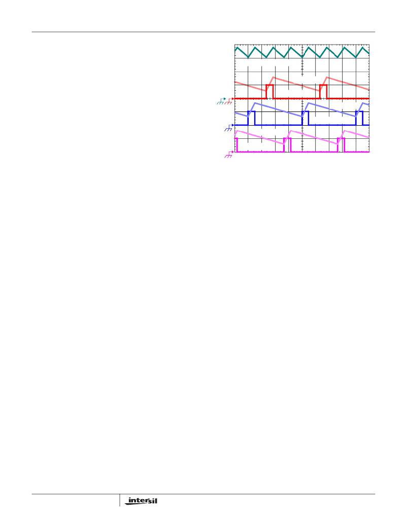
�IL1� +� IL2� +� IL3,� 7A/DIV�
�IL3,� 7A/DIV�
�PWM3,� 5V/DIV�
�IL2, 7A/DIV�
�PWM2,� 5V/DIV�
�IL1,� 7A/DIV�
�PWM1,� 5V/DIV�
�1μs/DIV�
�FIGURE� 1.� PWM� AND� INDUCTOR-CURRENT� WAVEFORMS�
�FOR� 3-PHASE� CONVERTER�
�Interleaving�
�The� switching� of� each� channel� in� a� multiphase� converter� is�
�timed� to� be� symmetrically� out� of� phase� with� each� of� the� other�
�channels.� In� a� 3-phase� converter,� each� channel� switches� 1/3�
�cycle� after� the� previous� channel� and� 1/3� cycle� before� the�
�following� channel.� As� a� result,� the� three-phase� converter� has�
�a� combined� ripple� frequency� three� times� greater� than� the�
�ripple� frequency� of� any� one� phase.� In� addition,� the� peak-to-�
�peak� amplitude� of� the� combined� inductor� currents� is� reduced�
�in� proportion� to� the� number� of� phases� (Equations� 1� and� 2).�
�Increased� ripple� frequency� and� lower� ripple� amplitude� mean�
�that� the� designer� can� use� less� per-channel� inductance� and�
�lower� total� output� capacitance� for� any� performance�
�specification.�
�Figure� 1� illustrates� the� multiplicative� effect� on� output� ripple�
�frequency.� The� three� channel� currents� (IL1,� IL2,� and� IL3)�
�combine� to� form� the� AC� ripple� current� and� the� DC� load�
�current.� The� ripple� component� has� three� times� the� ripple�
�frequency� of� each� individual� channel� current.� Each� PWM�
�pulse� is� terminated� 1/3� of� a� cycle� after� the� PWM� pulse� of� the�
�previous� phase.� The� peak-to-peak� current� for� each� phase� is�
�about� 7A,� and� the� DC� components� of� the� inductor� currents�
�combine� to� feed� the� load.�
�To� understand� the� reduction� of� ripple� current� amplitude� in� the�
�multiphase� circuit,� examine� the� equation� representing� an�
�individual� channel’s� peak-to-peak� inductor� current.�
�(� V� IN� –� V� OUT� )� V� OUT�
�are� impossible� to� ignore.� The� technical� challenges�
�associated� with� producing� a� single-phase� converter� which� is�
�both� cost-effective� and� thermally� viable� have� forced� a�
�I� PP� =� ------------------------------------------------------�
�L� f� S� V� IN�
�(EQ.� 1)�
�change� to� the� cost-saving� approach� of� multiphase.� The�
�ISL6564A� controller� helps� reduce� the� complexity� of�
�implementation� by� integrating� vital� functions� and� requiring�
�minimal� output� components.� The� block� diagrams� on� pages�
�3,� 4,� 5,� 6,� and� 7� provide� top� level� views� of� multiphase� power�
�conversion� using� the� ISL6564A� controller.�
�11�
�In� Equation� 1,� V� IN� and� V� OUT� are� the� input� and� output�
�voltages� respectively,� L� is� the� single-channel� inductor� value,�
�and� f� S� is� the� switching� frequency.�
�FN6285.1�
�March� 20,� 2007�
�相关PDF资料 |
PDF描述 |
|---|---|
| ISL6564IR-T | IC REG CTRLR BUCK PWM VM 40-QFN |
| ISL6565BCV-T | IC REG CTRLR BUCK PWM VM 28TSSOP |
| ISL6566AIRZ | IC CTRLR PWM 3PHASE BUCK 40-QFN |
| ISL6566CRZ-T | IC CTLR PWM BUCK 3PHASE 40-QFN |
| ISL6567CRZ | IC REG CTRLR BUCK PWM VM 24-QFN |
相关代理商/技术参数 |
参数描述 |
|---|---|
| ISL6564AIRZ-T | 功能描述:IC REG CTRLR BUCK PWM VM 40-QFN RoHS:是 类别:集成电路 (IC) >> PMIC - 稳压器 - DC DC 切换控制器 系列:- 产品培训模块:Lead (SnPb) Finish for COTS Obsolescence Mitigation Program 标准包装:2,500 系列:- PWM 型:电流模式 输出数:1 频率 - 最大:275kHz 占空比:50% 电源电压:18 V ~ 110 V 降压:无 升压:无 回扫:无 反相:无 倍增器:无 除法器:无 Cuk:无 隔离:是 工作温度:-40°C ~ 85°C 封装/外壳:8-SOIC(0.154",3.90mm 宽) 包装:带卷 (TR) |
| ISL6564CR | 功能描述:IC REG CTRLR BUCK PWM VM 40-QFN RoHS:否 类别:集成电路 (IC) >> PMIC - 稳压器 - DC DC 切换控制器 系列:- 标准包装:4,000 系列:- PWM 型:电压模式 输出数:1 频率 - 最大:1.5MHz 占空比:66.7% 电源电压:4.75 V ~ 5.25 V 降压:是 升压:无 回扫:无 反相:无 倍增器:无 除法器:无 Cuk:无 隔离:无 工作温度:-40°C ~ 85°C 封装/外壳:40-VFQFN 裸露焊盘 包装:带卷 (TR) |
| ISL6564CR-T | 功能描述:IC REG CTRLR BUCK PWM VM 40-QFN RoHS:否 类别:集成电路 (IC) >> PMIC - 稳压器 - DC DC 切换控制器 系列:- 标准包装:4,000 系列:- PWM 型:电压模式 输出数:1 频率 - 最大:1.5MHz 占空比:66.7% 电源电压:4.75 V ~ 5.25 V 降压:是 升压:无 回扫:无 反相:无 倍增器:无 除法器:无 Cuk:无 隔离:无 工作温度:-40°C ~ 85°C 封装/外壳:40-VFQFN 裸露焊盘 包装:带卷 (TR) |
| ISL6564CRZ | 功能描述:电流型 PWM 控制器 LEAD-FREE MULTI-PHASE PWM CONTROLLER W/ 0.525-1.3 VID RoHS:否 制造商:Texas Instruments 开关频率:27 KHz 上升时间: 下降时间: 工作电源电压:6 V to 15 V 工作电源电流:1.5 mA 输出端数量:1 最大工作温度:+ 105 C 安装风格:SMD/SMT 封装 / 箱体:TSSOP-14 |
| ISL6564CRZ-T | 功能描述:电流型 PWM 控制器 LEAD-FREE MULTI-PHASE PWM CONTROLLER W/ 0.525-1.3 VID, T&R RoHS:否 制造商:Texas Instruments 开关频率:27 KHz 上升时间: 下降时间: 工作电源电压:6 V to 15 V 工作电源电流:1.5 mA 输出端数量:1 最大工作温度:+ 105 C 安装风格:SMD/SMT 封装 / 箱体:TSSOP-14 |
发布紧急采购,3分钟左右您将得到回复。