参数资料
| 型号: | ISL6564AIRZ |
| 厂商: | Intersil |
| 文件页数: | 26/28页 |
| 文件大小: | 0K |
| 描述: | IC REG CTRLR BUCK PWM VM 40-QFN |
| 标准包装: | 500 |
| PWM 型: | 电压模式 |
| 输出数: | 1 |
| 频率 - 最大: | 1.5MHz |
| 占空比: | 66.7% |
| 电源电压: | 4.75 V ~ 5.25 V |
| 降压: | 是 |
| 升压: | 无 |
| 回扫: | 无 |
| 反相: | 无 |
| 倍增器: | 无 |
| 除法器: | 无 |
| Cuk: | 无 |
| 隔离: | 无 |
| 工作温度: | -40°C ~ 85°C |
| 封装/外壳: | 40-VFQFN 裸露焊盘 |
| 包装: | 管件 |
第1页第2页第3页第4页第5页第6页第7页第8页第9页第10页第11页第12页第13页第14页第15页第16页第17页第18页第19页第20页第21页第22页第23页第24页第25页当前第26页第27页第28页
�� �
�
�ISL6564A�
�and� off.� Select� low� ESL� ceramic� capacitors� and� place� one� as�
�close� as� possible� to� each� upper� MOSFET� drain� to� minimize�
�board� parasitic� impedances� and� maximize� suppression.�
�Layout� Considerations�
�The� following� layout� strategies� are� intended� to� minimize� the�
�impact� of� board� parasitic� impedances� on� converter�
�0.3�
�I� L,PP� =� 0�
�I� L,PP� =� 0.25� I� O�
�I� L,PP� =� 0.5� I� O�
�I� L,PP� =� 0.75� I� O�
�performance� and� to� optimize� the� heat-dissipating� capabilities�
�of� the� printed-circuit� board.� These� sections� highlight� some�
�important� practices� which� should� not� be� overlooked� during� the�
�layout� process.�
�0.2�
�0.1�
�Component� Placement�
�Within� the� allotted� implementation� area,� orient� the� switching�
�components� first.� The� switching� components� are� the� most�
�critical� because� they� carry� large� amounts� of� energy� and� tend�
�to� generate� high� levels� of� noise.� Switching� component�
�placement� should� take� into� account� power� dissipation.� Align�
�the� output� inductors� and� MOSFETs� such� that� space� between�
�the� components� is� minimized� while� creating� the� PHASE�
�plane.� Place� the� Intersil� MOSFET� driver� IC� as� close� as�
�0�
�0�
�0.2�
�0.4�
�0.6�
�0.8�
�1.0�
�possible� to� the� MOSFETs� they� control� to� reduce� the� parasitic�
�DUTY� CYCLE� (V� O/� V� IN� )�
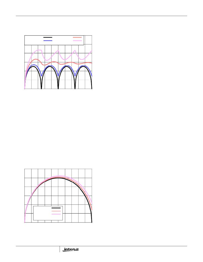
�FIGURE� 23.� NORMALIZED� INPUT-CAPACITOR� RMS� CURRENT�
�vs� DUTY� CYCLE� FOR� 4-PHASE� CONVERTER�
�MULTIPHASE� RMS� IMPROVEMENT�
�Figure� 24� is� provided� as� a� reference� to� demonstrate� the�
�dramatic� reductions� in� input-capacitor� RMS� current� upon� the�
�implementation� of� the� multiphase� topology.� For� example,�
�compare� the� input� RMS� current� requirements� of� a� two-phase�
�converter� versus� that� of� a� single� phase.� Assume� both�
�converters� have� a� duty� cycle� of� 0.25,� maximum� sustained�
�output� current� of� 40A,� and� a� ratio� of� I� L,PP� to� I� O� of� 0.5.� The�
�single� phase� converter� would� require� 17.3� Arms� current�
�capacity� while� the� two-phase� converter� would� only� require�
�10.9� Arms.� The� advantages� become� even� more� pronounced�
�when� output� current� is� increased� and� additional� phases� are�
�added� to� keep� the� component� cost� down� relative� to� the�
�single� phase� approach.�
�0.6�
�0.4�
�0.2�
�I� L,PP� =� 0�
�I� L,PP� =� 0.5� I� O�
�I� L,PP� =� 0.75� I� O�
�impedances� due� to� trace� length� between� critical� driver� input�
�and� output� signals.� If� possible,� duplicate� the� same�
�placement� of� these� components� for� each� phase.�
�Next,� place� the� input� and� output� capacitors.� Position� one�
�high-frequency� ceramic� input� capacitor� next� to� each� upper�
�MOSFET� drain.� Place� the� bulk� input� capacitors� as� close� to�
�the� upper� MOSFET� drains� as� dictated� by� the� component�
�size� and� dimensions.� Long� distances� between� input�
�capacitors� and� MOSFET� drains� result� in� too� much� trace�
�inductance� and� a� reduction� in� capacitor� performance.� Locate�
�the� output� capacitors� between� the� inductors� and� the� load,�
�while� keeping� them� in� close� proximity� to� the� microprocessor�
�socket.�
�The� ISL6564A� can� be� placed� off� to� one� side� or� centered�
�relative� to� the� individual� phase� switching� components.�
�Routing� of� sense� lines� and� PWM� signals� will� guide� final�
�placement.� Critical� small� signal� components� to� place� close�
�to� the� controller� include� the� ISEN� resistors,� R� T� resistor,�
�feedback� resistor,� and� compensation� components.�
�Bypass� capacitors� for� the� ISL6564A� and� ISL66XX� driver�
�bias� supplies� must� be� placed� next� to� their� respective� pins.�
�Trace� parasitic� impedances� will� reduce� their� effectiveness.�
�Plane� Allocation� and� Routing�
�Dedicate� one� solid� layer,� usually� a� middle� layer,� for� a� ground�
�plane.� Make� all� critical� component� ground� connections� with�
�vias� to� this� plane.� Dedicate� one� additional� layer� for� power�
�planes;� breaking� the� plane� up� into� smaller� islands� of�
�common� voltage.� Use� the� remaining� layers� for� signal� wiring.�
�Route� phase� planes� of� copper� filled� polygons� on� the� top� and�
�bottom� once� the� switching� component� placement� is� set.� Size�
�0�
�0�
�0.2�
�0.4�
�0.6�
�0.8�
�1.0�
�the� trace� width� between� the� driver� gate� pins� and� the�
�DUTY� CYCLE� (V� O/� V� IN� )�
�FIGURE� 24.� NORMALIZED� INPUT-CAPACITOR� RMS�
�CURRENT� vs� DUTY� CYCLE� FOR� SINGLE-PHASE�
�CONVERTER�
�26�
�MOSFET� gates� to� carry� 4A� of� current.� When� routing�
�components� in� the� switching� path,� use� short� wide� traces� to�
�reduce� the� associated� parasitic� impedances.�
�FN6285.1�
�March� 20,� 2007�
�相关PDF资料 |
PDF描述 |
|---|---|
| ISL6564IR-T | IC REG CTRLR BUCK PWM VM 40-QFN |
| ISL6565BCV-T | IC REG CTRLR BUCK PWM VM 28TSSOP |
| ISL6566AIRZ | IC CTRLR PWM 3PHASE BUCK 40-QFN |
| ISL6566CRZ-T | IC CTLR PWM BUCK 3PHASE 40-QFN |
| ISL6567CRZ | IC REG CTRLR BUCK PWM VM 24-QFN |
相关代理商/技术参数 |
参数描述 |
|---|---|
| ISL6564AIRZ-T | 功能描述:IC REG CTRLR BUCK PWM VM 40-QFN RoHS:是 类别:集成电路 (IC) >> PMIC - 稳压器 - DC DC 切换控制器 系列:- 产品培训模块:Lead (SnPb) Finish for COTS Obsolescence Mitigation Program 标准包装:2,500 系列:- PWM 型:电流模式 输出数:1 频率 - 最大:275kHz 占空比:50% 电源电压:18 V ~ 110 V 降压:无 升压:无 回扫:无 反相:无 倍增器:无 除法器:无 Cuk:无 隔离:是 工作温度:-40°C ~ 85°C 封装/外壳:8-SOIC(0.154",3.90mm 宽) 包装:带卷 (TR) |
| ISL6564CR | 功能描述:IC REG CTRLR BUCK PWM VM 40-QFN RoHS:否 类别:集成电路 (IC) >> PMIC - 稳压器 - DC DC 切换控制器 系列:- 标准包装:4,000 系列:- PWM 型:电压模式 输出数:1 频率 - 最大:1.5MHz 占空比:66.7% 电源电压:4.75 V ~ 5.25 V 降压:是 升压:无 回扫:无 反相:无 倍增器:无 除法器:无 Cuk:无 隔离:无 工作温度:-40°C ~ 85°C 封装/外壳:40-VFQFN 裸露焊盘 包装:带卷 (TR) |
| ISL6564CR-T | 功能描述:IC REG CTRLR BUCK PWM VM 40-QFN RoHS:否 类别:集成电路 (IC) >> PMIC - 稳压器 - DC DC 切换控制器 系列:- 标准包装:4,000 系列:- PWM 型:电压模式 输出数:1 频率 - 最大:1.5MHz 占空比:66.7% 电源电压:4.75 V ~ 5.25 V 降压:是 升压:无 回扫:无 反相:无 倍增器:无 除法器:无 Cuk:无 隔离:无 工作温度:-40°C ~ 85°C 封装/外壳:40-VFQFN 裸露焊盘 包装:带卷 (TR) |
| ISL6564CRZ | 功能描述:电流型 PWM 控制器 LEAD-FREE MULTI-PHASE PWM CONTROLLER W/ 0.525-1.3 VID RoHS:否 制造商:Texas Instruments 开关频率:27 KHz 上升时间: 下降时间: 工作电源电压:6 V to 15 V 工作电源电流:1.5 mA 输出端数量:1 最大工作温度:+ 105 C 安装风格:SMD/SMT 封装 / 箱体:TSSOP-14 |
| ISL6564CRZ-T | 功能描述:电流型 PWM 控制器 LEAD-FREE MULTI-PHASE PWM CONTROLLER W/ 0.525-1.3 VID, T&R RoHS:否 制造商:Texas Instruments 开关频率:27 KHz 上升时间: 下降时间: 工作电源电压:6 V to 15 V 工作电源电流:1.5 mA 输出端数量:1 最大工作温度:+ 105 C 安装风格:SMD/SMT 封装 / 箱体:TSSOP-14 |
发布紧急采购,3分钟左右您将得到回复。