参数资料
| 型号: | ISL6567CRZ |
| 厂商: | Intersil |
| 文件页数: | 13/25页 |
| 文件大小: | 0K |
| 描述: | IC REG CTRLR BUCK PWM VM 24-QFN |
| 标准包装: | 75 |
| PWM 型: | 电压模式 |
| 输出数: | 1 |
| 频率 - 最大: | 1.5MHz |
| 占空比: | 66% |
| 电源电压: | 4.9 V ~ 5.5 V |
| 降压: | 是 |
| 升压: | 无 |
| 回扫: | 无 |
| 反相: | 无 |
| 倍增器: | 无 |
| 除法器: | 无 |
| Cuk: | 无 |
| 隔离: | 无 |
| 工作温度: | 0°C ~ 70°C |
| 封装/外壳: | 24-VFQFN 裸露焊盘 |
| 包装: | 管件 |
| 产品目录页面: | 1243 (CN2011-ZH PDF) |
�� �
�
�ISL6567�
�minimal� impact� on� the� output� voltage� setting,� follow� the�
�V� REF�
�ISL6567�
�EXTERNAL� CIRCUIT�
�guidelines� presented� in� “Setting� the� Output� Voltage”� on�
��ERROR�
�AMPLIFIER�
�+�
�-�
�FB�
�R� S� (R� 1� )�
�R� P�
�+�
�To� V� OUT�
�EXTERNAL� REFERENCE� OPERATION�
�The� ISL6567� is� capable� of� accepting� an� external� voltage� and�
�using� it� as� a� reference� for� its� output� regulation.� To� enable� this�
�mode� of� operation,� the� MON� pin� potential� has� to� be� below� 3.5V�
�and� the� reference� voltage� has� to� be� connected� to� the� REFTRK�
�VDIFF�
�pin.� The� internal� or� external� reference� mode� of� operation� is�
�latched� in� every� time� the� POR� is� released� or� the� ISL6567� is�
�enabled.� The� highest� magnitude� external� reference� fed� to� the�
�REFTRK� pin� that� the� ISL6567� can� follow� is� limited� to� 2.3V.� The�
�X1�
�DIFFERENTIAL�
�AMPLIFIER�
�+�
�-�
�VSEN�
�RGND�
�ISL6567� utilizes� a� small� initial� negative� offset� (typically� about�
�50mV)� in� the� voltage� loop� at� the� beginning� of� it� soft-start,� to�
�counteract� any� positive� offsets� that� may� have� undesirable�
�effects.� As� this� initial� offset� is� phased� out� as� the� reference� is�
�ramped� up� to� around� 200mV,� in� order� to� avoid� an� error� in� the�
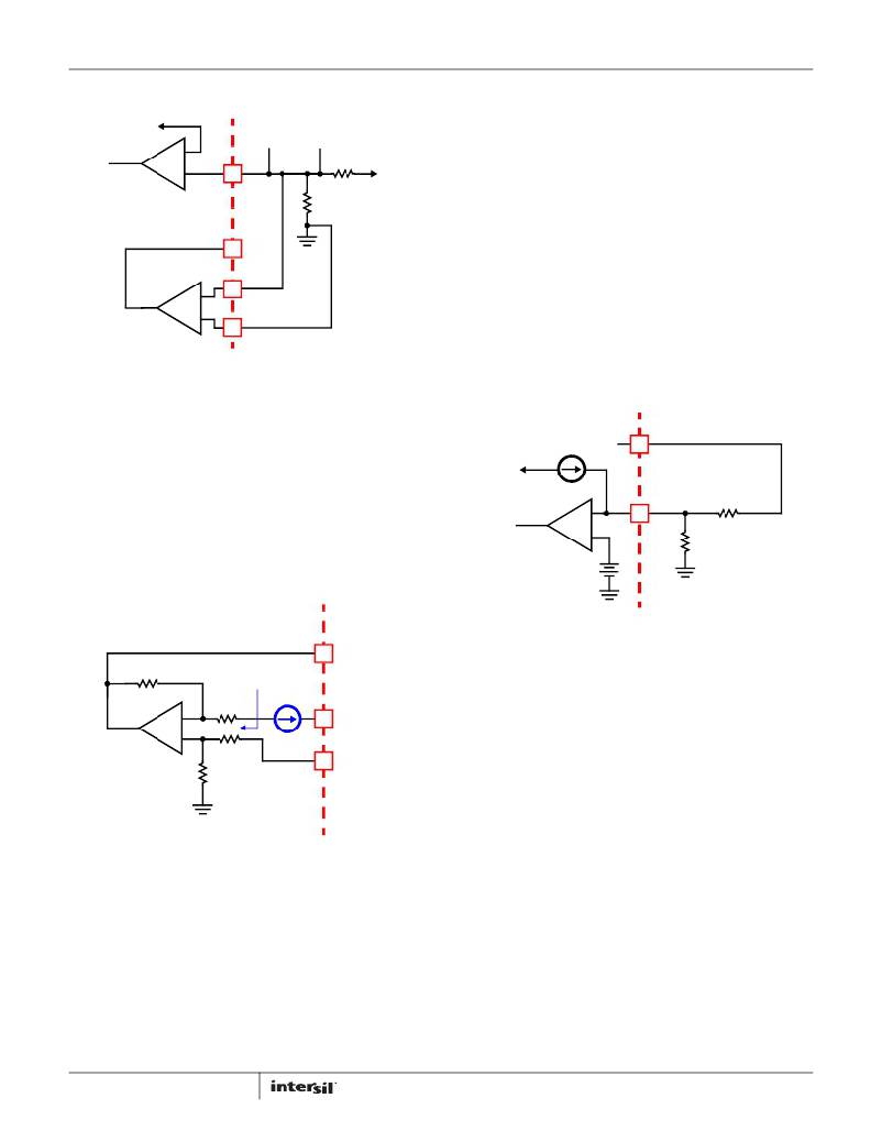
�FIGURE� 9.� SETTING� THE� OUTPUT� VOLTAGE� AT� THE� FB� PIN�
�output� regulation� level,� it� is� recommended� the� external�
�reference� has� an� amplitude� (final,� DC� level)� exceeding� 300mV.�
�The� differential� amplifier� can� be� used� even� if� remote� output�
�sensing� is� not� desired� or� not� feasible,� simply� connect� RGND� to�
�the� local� ground� and� connect� VSEN� to� the� output� voltage� being�
�monitored.� Should� one� desire� to� bypass� the� differential�
�VCC�
�I� H�
�(10μA)�
�ISL6567�
�EXTERNAL� CIRCUIT�
�VDIFF�
�amplifier,� the� circuit� in� Figure� 9� is� recommended� as� the� proper�
�-�
�implementation.� Since� its� output� is� monitored� for� OVP� and�
�PGOOD� purposes,� the� differential� amplifier� needs� to� be�
�connected� to� the� feedback� circuit� at� all� times,� hence� its� input�
�connections� to� FB� and� local� ground.� However,� its� output,� VDIFF,�
�can� be� left� open.� The� resistor� divider� setting� the� output� voltage�
�is� calculated� in� a� manner� identical� to� that� already� revealed.�
�ISL6567�
�EXTERNAL�
�+�
�MON�
�COMPARATOR�
�V� REF�
�(300mV)�
�+�
�-�
�MON�
�R� P�
�R� S�
�CIRCUIT�
�FIGURE� 11.� SETTING� THE� MONITORING� THRESHOLD� AND�
�VDIFF�
�HYSTERESIS�
�DIFFERENTIAL�
�AMPLIFIER�
�-�
�+�
�Z� IN�
�~2μA�
�VSEN�
�RGND�
�While� in� external� reference� (ER)� mode,� the� threshold� sensitive�
�MON� pin� can� be� used� to� control� when� the� ISL6567� starts� to�
�monitor� the� output� for� PGOOD� and� OVP� protection� purposes.�
�As� shown� in� Figure� 11,� connect� the� MON� pin� to� the� voltage� to�
�be� monitored� via� a� resistor� divider.� An� internal� current� source�
�helps� set� a� user-adjustable� monitor� threshold� hysteresis.�
�Choose� resistor� values� according� to� desired� hysteresis� voltage,�
�I� H�
�V� T� –� V� REF�
�Z� IN� > 240k� Ω�
�OVER� PROCESS,� TEMPERATURE,� AND�
�0� <� VSEN-RGND� <� 2.5V�
�FIGURE� 10.� SETTING� THE� OUTPUT� VOLTAGE� AT� THE� INPUT� OF�
�THE� DIFFERENTIAL� AMPLIFIER�
�DIFFERENTIAL� AMPLIFIER’S� UNITY� GAIN� NETWORK�
�The� differential� amplifier� on� the� ISL6567� utilizes� a� typical�
�resistive� network� along� with� active� compensating� circuitry� to�
�set� its� unity� gain.� This� resistive� network� can� affect� the� DC�
�regulation� setpoint� in� proportion� to� its� relative� magnitude�
�compared� to� the� external� output� voltage� setting� resistor�
�divider.� Figure� 10� details� the� internal� resistive� network.� For�
�13�
�V� H� ,� and� desired� rising� threshold,� V� T� .� Make� note� that,� in� these�
�equations,� V� REF� refers� to� the� reference� of� the� MON� comparator�
�(300mV).�
�V� H� R� S� ?� V� REF� (EQ.� 9)�
�R� S� =� ------� R� P� =� -------------------------�
�Intersil� recommends� the� MON� threshold� is� set� to� be� tripped�
�when� the� external� reference� voltage� reaches� at� least� 90%� of�
�the� final� DC� value.� Since� PGOOD� and� OVP� monitoring� are�
�relative� to� the� external� reference� magnitude,� it� is� important� to�
�understand� that� the� PGOOD� and� OVP� thresholds� will� move� in�
�proportion� to� the� moving� reference� (externally� soft-started�
�reference).� Thus,� the� absolute� thresholds� of� PGOOD� and� OVP.�
�FN9243.4�
�August� 9,� 2011�
�相关PDF资料 |
PDF描述 |
|---|---|
| ISL6568CRZ-T | IC CTLR PWM BUCK 2PHASE 32-QFN |
| ISL6569ACR-T | IC REG CTRLR BUCK PWM 32-QFN |
| ISL6569CR-T | IC REG CTRLR DIVIDER PWM 32-QFN |
| ISL6571CRZ | IC MOSF DRVR/SYNC SW COMPL 68QFN |
| ISL6611AIRZ | IC REG CTRLR DOUBLER PWM 16-QFN |
相关代理商/技术参数 |
参数描述 |
|---|---|
| ISL6567CRZ-T | 功能描述:IC REG CTRLR BUCK PWM VM 24-QFN RoHS:是 类别:集成电路 (IC) >> PMIC - 稳压器 - DC DC 切换控制器 系列:- 产品培训模块:Lead (SnPb) Finish for COTS Obsolescence Mitigation Program 标准包装:2,500 系列:- PWM 型:电流模式 输出数:1 频率 - 最大:275kHz 占空比:50% 电源电压:18 V ~ 110 V 降压:无 升压:无 回扫:无 反相:无 倍增器:无 除法器:无 Cuk:无 隔离:是 工作温度:-40°C ~ 85°C 封装/外壳:8-SOIC(0.154",3.90mm 宽) 包装:带卷 (TR) |
| ISL6567IRZ | 功能描述:IC REG CTRLR BUCK PWM VM 24-QFN RoHS:是 类别:集成电路 (IC) >> PMIC - 稳压器 - DC DC 切换控制器 系列:- 产品培训模块:Lead (SnPb) Finish for COTS Obsolescence Mitigation Program 标准包装:2,500 系列:- PWM 型:电流模式 输出数:1 频率 - 最大:275kHz 占空比:50% 电源电压:18 V ~ 110 V 降压:无 升压:无 回扫:无 反相:无 倍增器:无 除法器:无 Cuk:无 隔离:是 工作温度:-40°C ~ 85°C 封装/外壳:8-SOIC(0.154",3.90mm 宽) 包装:带卷 (TR) |
| ISL6567IRZS2698 | 功能描述:IC REG CTRLR BUCK PWM VM 24-QFN RoHS:是 类别:集成电路 (IC) >> PMIC - 稳压器 - DC DC 切换控制器 系列:- 产品培训模块:Lead (SnPb) Finish for COTS Obsolescence Mitigation Program 标准包装:2,500 系列:- PWM 型:电流模式 输出数:1 频率 - 最大:275kHz 占空比:50% 电源电压:18 V ~ 110 V 降压:无 升压:无 回扫:无 反相:无 倍增器:无 除法器:无 Cuk:无 隔离:是 工作温度:-40°C ~ 85°C 封装/外壳:8-SOIC(0.154",3.90mm 宽) 包装:带卷 (TR) |
| ISL6567IRZ-T | 功能描述:IC REG CTRLR BUCK PWM VM 24-QFN RoHS:是 类别:集成电路 (IC) >> PMIC - 稳压器 - DC DC 切换控制器 系列:- 产品培训模块:Lead (SnPb) Finish for COTS Obsolescence Mitigation Program 标准包装:2,500 系列:- PWM 型:电流模式 输出数:1 频率 - 最大:275kHz 占空比:50% 电源电压:18 V ~ 110 V 降压:无 升压:无 回扫:无 反相:无 倍增器:无 除法器:无 Cuk:无 隔离:是 工作温度:-40°C ~ 85°C 封装/外壳:8-SOIC(0.154",3.90mm 宽) 包装:带卷 (TR) |
| ISL6567IRZ-TS2698 | 功能描述:IC REG CTRLR BUCK PWM VM 24-QFN RoHS:是 类别:集成电路 (IC) >> PMIC - 稳压器 - DC DC 切换控制器 系列:- 产品培训模块:Lead (SnPb) Finish for COTS Obsolescence Mitigation Program 标准包装:2,500 系列:- PWM 型:电流模式 输出数:1 频率 - 最大:275kHz 占空比:50% 电源电压:18 V ~ 110 V 降压:无 升压:无 回扫:无 反相:无 倍增器:无 除法器:无 Cuk:无 隔离:是 工作温度:-40°C ~ 85°C 封装/外壳:8-SOIC(0.154",3.90mm 宽) 包装:带卷 (TR) |
发布紧急采购,3分钟左右您将得到回复。