参数资料
| 型号: | ISL6567CRZ |
| 厂商: | Intersil |
| 文件页数: | 18/25页 |
| 文件大小: | 0K |
| 描述: | IC REG CTRLR BUCK PWM VM 24-QFN |
| 标准包装: | 75 |
| PWM 型: | 电压模式 |
| 输出数: | 1 |
| 频率 - 最大: | 1.5MHz |
| 占空比: | 66% |
| 电源电压: | 4.9 V ~ 5.5 V |
| 降压: | 是 |
| 升压: | 无 |
| 回扫: | 无 |
| 反相: | 无 |
| 倍增器: | 无 |
| 除法器: | 无 |
| Cuk: | 无 |
| 隔离: | 无 |
| 工作温度: | 0°C ~ 70°C |
| 封装/外壳: | 24-VFQFN 裸露焊盘 |
| 包装: | 管件 |
| 产品目录页面: | 1243 (CN2011-ZH PDF) |
�� �
�
�ISL6567�
�through� 20� assume� a� VCC� voltage� of� 5V,� the� design� aid� curves�
�(optional)�
�can� be� translated� to� a� different� VCC� voltage� by� translating�
�them� in� the� amount� of� the� voltage� differential,� to� the� left� for� a�
�lower� VCC� voltage,� or� to� the� right� for� a� higher� VCC� voltage.�
�Should� the� simple� series� bias� resistor� configuration� fall� short�
�of� providing� the� necessary� bias� current,� the� internal� shunt�
�regulator� can� be� used� in� conjunction� with� an� external� BJT�
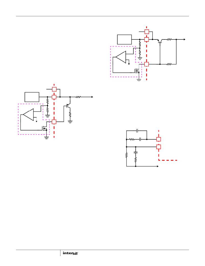
�transistor� to� increase� the� shunt� regulator� current.� Figure� 21�
�details� such� an� implementation� utilizing� a� PNP� transistor.�
�E/A�
�POR�
�CIRCUIT�
�-�
�ISL6567�
�EXTERNAL� CIRCUIT�
�PVCC�
�Q1�
�R1�
�VCC�
�V� IN�
�Selection� of� R� 1� can� be� based� on� the� graphs� provided� for� the�
�passive� regulator� configuration.� Maximum� power� dissipation�
�+�
�inside� Q� 1� will� take� place� when� maximum� voltage� is� applied� to�
�the� circuit� and� the� ISL6567� is� disabled;� determine� I� VREGMAX�
�by� reverse-use� of� the� graph� in� Figure� 18� and� use� the� obtained�
�number� to� calculate� Q� 1� power� dissipation.�
�ISL6567�
�EXTERNAL� CIRCUIT�
�VREF�
�SHUNT� REGULATOR�
�VREG�
�R2�
�PVCC�
�V� IN�
�FIGURE� 22.� INTERNAL� SHUNT� REGULATOR� USE� WITH� EXTERNAL�
�NPN� TRANSISTOR� (ACTIVE� CONFIGURATION)�
�POR�
�CIRCUIT�
�VCC�
�Q1�
�R1�
�FREQUENCY� COMPENSATION�
�The� ISL6567� multi-phase� converter� behaves� in� a� similar�
�manner� to� a� voltage-mode� controller.� This� section� highlights� the�
�E/A�
�-�
�+�
�R2�
�(optional)�
�design� consideration� for� a� voltage-mode� controller� requiring�
�external� compensation.� To� address� a� broad� range� of�
�applications,� a� type-3� feedback� network� is� recommended� (see�
�VREF�
�VREG�
�Figure� 23).�
�C2�
�SHUNT� REGULATOR�
�FIGURE� 21.� INTERNAL� SHUNT� REGULATOR� USE� WITH� EXTERNAL�
�PNP� TRANSISTOR� (ACTIVE� CONFIGURATION)�
�R1�
�R2�
�C1�
�C3�
�COMP�
�FB�
�ISL6567�
�An� NPN� transistor� can� also� be� used� to� increase� the� maximum�
�available� bias� current,� as� shown� in� Figure� 22.� Used� as� a� series�
�pass� element,� Q� 1� will� dissipate� the� most� power� when� the�
�circuit� is� enabled� and� operational,� and� the� input� voltage,� V� IN� ,� is�
�at� its� highest� level.�
�With� the� series� pass� element� configuration� shown� in�
�Figure� 22,� the� difference� between� the� input� and� the� regulation�
�level� at� the� VCC� pin� has� to� be� higher� than� the� lowest�
�acceptable� V� CE� of� Q� 1� (may� choose� to� run� Q� 1� into� saturation,�
�but� must� consider� the� reduced� gain).� Thus,� R� 2� has� to� be�
�chosen� such� that� it� will� provide� appropriate� base� current� at�
�lowest� V� CE� of� Q� 1� .� Next,� ensure� the� ISL6567’s� I� VREGMAX� is� not�
�exceeded� when� the� input� voltage� swings� to� its� highest� extreme�
�(assume� base� current� goes� to� 0� when� the� IC� is� disabled).� R� 1� is�
�an� optional� circuit� element:� it� can� be� added� to� offset� some� of�
�the� power� dissipation� in� Q� 1� ,� but� it� also� reduces� the� available�
�V� CE� for� Q� 1� .� If� utilizing� such� a� series� resistor,� check� that� it� does�
�not� impede� on� the� proper� operation� at� the� lowest� input� voltage�
�and� choose� a� power� rating� corresponding� to� the� highest� bias�
�current� that� the� ISL6567� may� require� to� drive� the� switching�
�MOSFETs.�
�18�
�R3�
�V� DIFF� (V� OUT� )�
�FIGURE� 23.� COMPENSATION� CONFIGURATION� FOR� ISL6567�
�CIRCUIT�
�Figure� 24� highlights� the� voltage-mode� control� loop� for� a�
�synchronous-rectified� buck� converter,� applicable,� with� a� small�
�number� of� adjustments,� to� the� multi-phase� ISL6567� circuit.� The�
�output� voltage� (V� OUT� )� is� regulated� to� the� reference� voltage,� VREF,�
�level.� The� error� amplifier� output� (COMP� pin� voltage)� is� compared�
�with� the� oscillator� (OSC)� modified� saw-tooth� wave� to� provide� a�
�pulse-width� modulated� wave� with� an� amplitude� of� V� IN� at� the�
�PHASE� node.� The� PWM� wave� is� smoothed� by� the� output� filter�
�(L� and� C).� The� output� filter� capacitor� bank’s� equivalent� series�
�resistance� is� represented� by� the� series� resistor� E.�
�FN9243.4�
�August� 9,� 2011�
�相关PDF资料 |
PDF描述 |
|---|---|
| ISL6568CRZ-T | IC CTLR PWM BUCK 2PHASE 32-QFN |
| ISL6569ACR-T | IC REG CTRLR BUCK PWM 32-QFN |
| ISL6569CR-T | IC REG CTRLR DIVIDER PWM 32-QFN |
| ISL6571CRZ | IC MOSF DRVR/SYNC SW COMPL 68QFN |
| ISL6611AIRZ | IC REG CTRLR DOUBLER PWM 16-QFN |
相关代理商/技术参数 |
参数描述 |
|---|---|
| ISL6567CRZ-T | 功能描述:IC REG CTRLR BUCK PWM VM 24-QFN RoHS:是 类别:集成电路 (IC) >> PMIC - 稳压器 - DC DC 切换控制器 系列:- 产品培训模块:Lead (SnPb) Finish for COTS Obsolescence Mitigation Program 标准包装:2,500 系列:- PWM 型:电流模式 输出数:1 频率 - 最大:275kHz 占空比:50% 电源电压:18 V ~ 110 V 降压:无 升压:无 回扫:无 反相:无 倍增器:无 除法器:无 Cuk:无 隔离:是 工作温度:-40°C ~ 85°C 封装/外壳:8-SOIC(0.154",3.90mm 宽) 包装:带卷 (TR) |
| ISL6567IRZ | 功能描述:IC REG CTRLR BUCK PWM VM 24-QFN RoHS:是 类别:集成电路 (IC) >> PMIC - 稳压器 - DC DC 切换控制器 系列:- 产品培训模块:Lead (SnPb) Finish for COTS Obsolescence Mitigation Program 标准包装:2,500 系列:- PWM 型:电流模式 输出数:1 频率 - 最大:275kHz 占空比:50% 电源电压:18 V ~ 110 V 降压:无 升压:无 回扫:无 反相:无 倍增器:无 除法器:无 Cuk:无 隔离:是 工作温度:-40°C ~ 85°C 封装/外壳:8-SOIC(0.154",3.90mm 宽) 包装:带卷 (TR) |
| ISL6567IRZS2698 | 功能描述:IC REG CTRLR BUCK PWM VM 24-QFN RoHS:是 类别:集成电路 (IC) >> PMIC - 稳压器 - DC DC 切换控制器 系列:- 产品培训模块:Lead (SnPb) Finish for COTS Obsolescence Mitigation Program 标准包装:2,500 系列:- PWM 型:电流模式 输出数:1 频率 - 最大:275kHz 占空比:50% 电源电压:18 V ~ 110 V 降压:无 升压:无 回扫:无 反相:无 倍增器:无 除法器:无 Cuk:无 隔离:是 工作温度:-40°C ~ 85°C 封装/外壳:8-SOIC(0.154",3.90mm 宽) 包装:带卷 (TR) |
| ISL6567IRZ-T | 功能描述:IC REG CTRLR BUCK PWM VM 24-QFN RoHS:是 类别:集成电路 (IC) >> PMIC - 稳压器 - DC DC 切换控制器 系列:- 产品培训模块:Lead (SnPb) Finish for COTS Obsolescence Mitigation Program 标准包装:2,500 系列:- PWM 型:电流模式 输出数:1 频率 - 最大:275kHz 占空比:50% 电源电压:18 V ~ 110 V 降压:无 升压:无 回扫:无 反相:无 倍增器:无 除法器:无 Cuk:无 隔离:是 工作温度:-40°C ~ 85°C 封装/外壳:8-SOIC(0.154",3.90mm 宽) 包装:带卷 (TR) |
| ISL6567IRZ-TS2698 | 功能描述:IC REG CTRLR BUCK PWM VM 24-QFN RoHS:是 类别:集成电路 (IC) >> PMIC - 稳压器 - DC DC 切换控制器 系列:- 产品培训模块:Lead (SnPb) Finish for COTS Obsolescence Mitigation Program 标准包装:2,500 系列:- PWM 型:电流模式 输出数:1 频率 - 最大:275kHz 占空比:50% 电源电压:18 V ~ 110 V 降压:无 升压:无 回扫:无 反相:无 倍增器:无 除法器:无 Cuk:无 隔离:是 工作温度:-40°C ~ 85°C 封装/外壳:8-SOIC(0.154",3.90mm 宽) 包装:带卷 (TR) |
发布紧急采购,3分钟左右您将得到回复。