- 您现在的位置:买卖IC网 > Datasheet目录334 > ISL6615AIBZ (Intersil)IC MOSFET DRVR SYNC HF 6A 8-SOIC Datasheet资料下载
参数资料
| 型号: | ISL6615AIBZ |
| 厂商: | Intersil |
| 文件页数: | 7/12页 |
| 文件大小: | 0K |
| 描述: | IC MOSFET DRVR SYNC HF 6A 8-SOIC |
| 标准包装: | 980 |
| 配置: | 高端和低端,同步 |
| 输入类型: | PWM |
| 延迟时间: | 10ns |
| 电流 - 峰: | 2.5A |
| 配置数: | 1 |
| 输出数: | 2 |
| 高端电压 - 最大(自引导启动): | 36V |
| 电源电压: | 6.8 V ~ 13.2 V |
| 工作温度: | -40°C ~ 70°C |
| 安装类型: | 表面贴装 |
| 封装/外壳: | 8-SOIC(0.154",3.90mm 宽) |
| 供应商设备封装: | 8-SOIC |
| 包装: | 管件 |
�� �
�
�ISL6615A�
�Power-On� Reset� (POR)� Function�
�During� initial� start-up,� the� VCC� voltage� rise� is� monitored.� Once� the�
�rising� VCC� voltage� exceeds� 6.4V� (typically),� operation� of� the� driver�
�is� enabled� and� the� PWM� input� signal� takes� control� of� the� gate�
�drives.� If� VCC� drops� below� the� falling� threshold� of� 5.0V� (typically),�
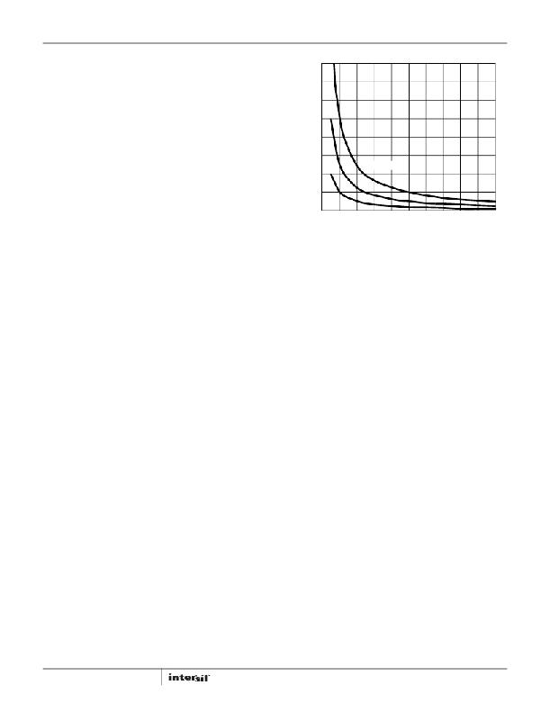
�1.6�
�1.4�
�1.2�
�operation� of� the� driver� is� disabled.�
�1.0�
�Pre-POR� Overvoltage� Protection�
�Prior� to� VCC� exceeding� its� POR� level,� the� upper� gate� is� held� low�
�0.8�
�and� the� lower� gate� is� controlled� by� the� overvoltage� protection�
�circuits.� The� upper� gate� driver� is� powered� from� PVCC� and� will� be�
�held� low� when� a� voltage� of� 2.75V� or� higher� is� present� on� PVCC� as�
�VCC� surpasses� its� POR� threshold.� The� PHASE� is� connected� to� the�
�gate� of� the� low� side� MOSFET� (LGATE),� which� provides� some�
�protection� to� the� microprocessor� if� the� upper� MOSFET(s)� is�
�0.6�
�0.4�
�0.2�
�20nC�
�Q� GATE� = 100nC�
�50nC�
�shorted� during� start-up,� normal,� or� shutdown� conditions.� For�
�complete� protection,� the� low� side� MOSFET� should� have� a� gate�
�threshold� well� below� the� maximum� voltage� rating� of� the�
�load/microprocessor.�
�0.0�
�0.0� 0.1� 0.2� 0.3� 0.4� 0.5� 0.6� 0.7� 0.8� 0.9�
�Δ� V� BOOT_CAP� (V)�
�FIGURE� 2.� BOOTSTRAP� CAPACITANCE� vs� BOOT� RIPPLE�
�VOLTAGE�
�1.0�
�Internal� Bootstrap� Device�
�Both� drivers� feature� an� internal� bootstrap� Schottky� diode.� Simply�
�adding� an� external� capacitor� across� the� BOOT� and� PHASE� pins�
�completes� the� bootstrap� circuit.� The� bootstrap� function� is� also�
�designed� to� prevent� the� bootstrap� capacitor� from� overcharging�
�due� to� the� large� negative� swing� at� the� trailing-edge� of� the� PHASE�
�node.� This� reduces� voltage� stress� on� the� boot� to� phase� pins.�
�The� bootstrap� capacitor� must� have� a� maximum� voltage� rating�
�above� PVCC� +� 5V� and� its� capacitance� value� can� be� chosen� from�
�Equation� 1:�
�Gate� Drive� Voltage� Versatility�
�The� ISL6615A� provides� the� user� with� flexibility� in� choosing� the�
�gate� drive� voltage� for� efficiency� optimization.� The� ISL6615A� ties�
�the� upper� and� lower� drive� rails� together.� Simply� applying� a�
�voltage� from� +4.5V� up� to� 13.2V� on� PVCC� sets� both� gate� drive� rail�
�voltages� simultaneously,� while� VCC’s� operating� range� is� from�
�+6.8V� up� to� 13.2V.�
�Power� Dissipation�
�Package� power� dissipation� is� mainly� a� function� of� the� switching�
�C� BOOT_CAP� ≥� ---------------------------------�
�Q� GATE�
�Δ� V� BOOT_CAP�
�(EQ.� 1)�
�frequency� (F� SW� ),� the� output� drive� impedance,� the� external� gate�
�resistance� and� the� selected� MOSFET’s� internal� gate� resistance� and�
�total� gate� charge.� Calculating� the� power� dissipation� in� the� driver� for�
�Q� GATE� =� -------------------------------� ?� N� Q1�
�Q� G1� ?� PVCC�
�V� GS1�
�where� Q� G1� is� the� amount� of� gate� charge� per� upper� MOSFET� at�
�V� GS1� gate-source� voltage� and� N� Q1� is� the� number� of� control�
�MOSFETs.� The� Δ� V� BOOT_CAP� term� is� defined� as� the� allowable�
�droop� in� the� rail� of� the� upper� gate� drive.�
�As� an� example,� suppose� two� IRLR7821� FETs� are� chosen� as� the�
�upper� MOSFETs.� The� gate� charge,� Q� G� ,� from� the� data� sheet� is�
�10nC� at� 4.5V� (V� GS� )� gate-source� voltage.� Then� the� Q� GATE� is�
�calculated� to� be� 53nC� for� PVCC� =� 12V.� We� will� assume� a� 200mV�
�droop� in� drive� voltage� over� the� PWM� cycle.� We� find� that� a�
�bootstrap� capacitance� of� at� least� 0.267μF� is� required.� The� next�
�larger� standard� value� capacitance� is� 0.33μF.� A� good� quality�
�ceramic� capacitor� is� recommended.�
�a� desired� application� is� critical� to� ensure� safe� operation.� Exceeding�
�the� maximum� allowable� power� dissipation� level� will� push� the� IC�
�beyond� the� maximum� recommended� operating� junction�
�temperature� of� +125°C.� The� maximum� allowable� IC� power�
�dissipation� for� the� SO8� package� is� approximately� 800mW� at� room�
�temperature,� while� the� power� dissipation� capacity� in� the� DFN�
�package� (with� an� exposed� heat� escape� pad)� is� more� than� 1.5W.� The�
�DFN� package� is� more� suitable� for� high� frequency� applications.� See�
�“Layout� Considerations”� on� page� 8� for� thermal� transfer�
�improvement� suggestions.� When� designing� the� driver� into� an�
�application,� it� is� recommended� that� the� following� calculation� is� used�
�to� ensure� safe� operation� at� the� desired� frequency� for� the� selected�
�MOSFETs.� The� total� gate� drive� power� losses� due� to� the� gate� charge�
�of� MOSFETs� and� the� driver’s� internal� circuitry� and� their�
�corresponding� average� driver� current� can� be� estimated� with�
�Equations� 2� and� 3,� respectively:�
�Q� G1� ?� PVCC� 2�
�P� Qg_Q1� =� -----------------------------------� ?� F� SW� ?� N� Q1�
�Q� G2� ?� PVCC� 2�
�P� Qg_Q2� =� -----------------------------------� ?� F� SW� ?� N� Q2�
�I� DR� =� ?� ------------------------------------------------� +� ------------------------------------------------� ?� ?� F� SW� +� I� Q�
�P� Qg_TOT� =� P� Qg_Q1� +� P� Qg_Q2� +� I� Q� ?� VCC�
�V� GS1�
�V� GS2�
�?� Q� G1� ?� PVCC� ?� N� Q1� Q� G2� ?� PVCC� ?� N� Q2� ?�
�?� V� GS1� V� GS2� ?�
�(EQ.� 2)�
�(EQ.� 3)�
�7�
�FN6608.2�
�April� 13,� 2012�
�相关PDF资料 |
PDF描述 |
|---|---|
| ISL6615IBZ | IC MOSFET DRVR SYNC HF 6A 8-SOIC |
| ISL6620ACBZ | IC SYNC RECT MOSFET DRVR 8-SOIC |
| ISL6622AIBZ | IC MOSFET DRVR SYNC BUCK 8-SOIC |
| ISL6622CBZ-T | IC MOSFET DVR SYNC BUCK 8-SOIC |
| ISL6801ABT | IC DRIVER HISIDE BOOTSTRAP 8SOIC |
相关代理商/技术参数 |
参数描述 |
|---|---|
| ISL6615AIBZ-T | 功能描述:IC MOSFET DRVR SYNC HF 6A 8-SOIC RoHS:是 类别:集成电路 (IC) >> PMIC - MOSFET,电桥驱动器 - 外部开关 系列:- 标准包装:50 系列:- 配置:高端 输入类型:非反相 延迟时间:200ns 电流 - 峰:250mA 配置数:1 输出数:1 高端电压 - 最大(自引导启动):600V 电源电压:12 V ~ 20 V 工作温度:-40°C ~ 125°C 安装类型:通孔 封装/外壳:8-DIP(0.300",7.62mm) 供应商设备封装:8-DIP 包装:管件 其它名称:*IR2127 |
| ISL6615AIRZ | 功能描述:IC MOSFET DRVR SYNC HF 6A 10-DFN RoHS:是 类别:集成电路 (IC) >> PMIC - MOSFET,电桥驱动器 - 外部开关 系列:- 标准包装:50 系列:- 配置:高端 输入类型:非反相 延迟时间:200ns 电流 - 峰:250mA 配置数:1 输出数:1 高端电压 - 最大(自引导启动):600V 电源电压:12 V ~ 20 V 工作温度:-40°C ~ 125°C 安装类型:通孔 封装/外壳:8-DIP(0.300",7.62mm) 供应商设备封装:8-DIP 包装:管件 其它名称:*IR2127 |
| ISL6615AIRZ-T | 功能描述:IC MOSFET DRVR SYNC HF 6A 10-DFN RoHS:是 类别:集成电路 (IC) >> PMIC - MOSFET,电桥驱动器 - 外部开关 系列:- 标准包装:50 系列:- 配置:高端 输入类型:非反相 延迟时间:200ns 电流 - 峰:250mA 配置数:1 输出数:1 高端电压 - 最大(自引导启动):600V 电源电压:12 V ~ 20 V 工作温度:-40°C ~ 125°C 安装类型:通孔 封装/外壳:8-DIP(0.300",7.62mm) 供应商设备封装:8-DIP 包装:管件 其它名称:*IR2127 |
| ISL6615CBZ | 功能描述:IC MOSFET DRVR SYNC HF 6A 8-SOIC RoHS:是 类别:集成电路 (IC) >> PMIC - MOSFET,电桥驱动器 - 外部开关 系列:- 标准包装:50 系列:- 配置:高端 输入类型:非反相 延迟时间:200ns 电流 - 峰:250mA 配置数:1 输出数:1 高端电压 - 最大(自引导启动):600V 电源电压:12 V ~ 20 V 工作温度:-40°C ~ 125°C 安装类型:通孔 封装/外壳:8-DIP(0.300",7.62mm) 供应商设备封装:8-DIP 包装:管件 其它名称:*IR2127 |
| ISL6615CBZ-T | 功能描述:IC MOSFET DRVR SYNC HF 6A 8-SOIC RoHS:是 类别:集成电路 (IC) >> PMIC - MOSFET,电桥驱动器 - 外部开关 系列:- 标准包装:6,000 系列:* |
发布紧急采购,3分钟左右您将得到回复。