- 您现在的位置:买卖IC网 > Datasheet目录334 > ISL6615AIBZ (Intersil)IC MOSFET DRVR SYNC HF 6A 8-SOIC Datasheet资料下载
参数资料
| 型号: | ISL6615AIBZ |
| 厂商: | Intersil |
| 文件页数: | 8/12页 |
| 文件大小: | 0K |
| 描述: | IC MOSFET DRVR SYNC HF 6A 8-SOIC |
| 标准包装: | 980 |
| 配置: | 高端和低端,同步 |
| 输入类型: | PWM |
| 延迟时间: | 10ns |
| 电流 - 峰: | 2.5A |
| 配置数: | 1 |
| 输出数: | 2 |
| 高端电压 - 最大(自引导启动): | 36V |
| 电源电压: | 6.8 V ~ 13.2 V |
| 工作温度: | -40°C ~ 70°C |
| 安装类型: | 表面贴装 |
| 封装/外壳: | 8-SOIC(0.154",3.90mm 宽) |
| 供应商设备封装: | 8-SOIC |
| 包装: | 管件 |
�� �
�
�ISL6615A�
�where� the� gate� charge� (Q� G1� and� Q� G2� )� is� defined� at� a� particular�
�gate� to� source� voltage� (V� GS1� and� V� GS2� )� in� the� corresponding�
�MOSFET� datasheet;� I� Q� is� the� driver’s� total� quiescent� current� with�
�no� load� at� both� drive� outputs;� N� Q1� and� N� Q2� are� the� number� of�
�upper� and� lower� MOSFETs,� respectively;� PVCC� is� the� drive� voltage�
�for� both� upper� and� lower� FETs.� The� I� Q� *VCC� product� is� the�
�quiescent� power� of� the� driver� without� capacitive� load� and� is�
�typically� 200mW� at� 300kHz� and� VCC� =� PVCC� =� 12V.�
�The� total� gate� drive� power� losses� are� dissipated� among� the�
�resistive� components� along� the� transition� path.� The� drive�
�resistance� dissipates� a� portion� of� the� total� gate� drive� power�
�losses;� the� rest� will� be� dissipated� by� the� external� gate� resistors�
�(R� G1� and� R� G2� )� and� the� internal� gate� resistors� (R� GI1� and� R� GI2� )� of�
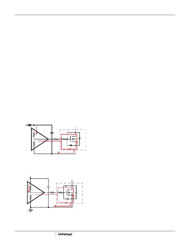
�MOSFETs.� Figures� 3� and� 4� show� the� typical� upper� and� lower� gate�
�drives� turn-on� transition� path.� The� power� dissipation� on� the� driver�
�can� be� roughly� estimated,� as� shown� in� Equation� 4.�
�Application� Information�
�Layout� Considerations�
�The� parasitic� inductances� of� the� PCB� and� of� the� power� devices’�
�packaging� (both� upper� and� lower� MOSFETs)� can� cause� serious�
�ringing,� exceeding� the� absolute� maximum� ratings� of� the� devices.�
�A� good� layout� helps� reduce� the� ringing� on� the� switching� node�
�(PHASE)� and� significantly� lowers� the� stress� applied� to� the� output�
�drives.� The� following� advice� is� meant� to� lead� to� an� optimized�
�layout� and� performance:�
�?� Keep� decoupling� loops� (VCC-GND,� PVCC-GND� and� BOOT-PHASE)�
�short� and� wide� (at� least� 25� mils).� Avoid� using� vias� on� decoupling�
�components� other� than� their� ground� terminals,� which� should� be�
�on� a� copper� plane� with� at� least� two� vias.�
�?� Minimize� trace� inductance,� especially� on� low-impedance� lines.�
�All� power� traces� (UGATE,� PHASE,� LGATE,� GND,� PVCC,� VCC,�
�P� DR_UP� =� ?� -----------------------------------� +� -------------------------------------� ?� ?� -------------------�
�?� R� HI1� +� R� EXT1� R� LO1� +� R� EXT1� ?�
�P� DR_LOW� =� ?� -----------------------------------� +� -------------------------------------� ?� ?� -------------------�
�R� HI2� +� R� EXT2� R� LO2� +� R� EXT2� ?�
�?�
�P� DR� =� P� DR_UP� +� P� DR_LOW� +� I� Q� ?� VCC�
�?� R� HI1� R� LO1� ?� P� Qg_Q1�
�2�
�?� R� HI2� R� LO2� ?� P� Qg_Q2�
�2�
�(EQ.� 4)�
�GND)� should� be� short� and� wide� (at� least� 25� mils).� Try� to� place�
�power� traces� on� a� single� layer,� otherwise,� two� vias� on�
�interconnection� are� preferred� where� possible.� For� no�
�connection� (NC)� pins� on� the� QFN� part,� connecting� them� to� the�
�adjacent� net� (LGATE2/PHASE2)� can� reduce� trace� inductance.�
�?� Shorten� all� gate� drive� loops� (UGATE-PHASE� and� LGATE-GND)�
�and� route� them� closely� spaced.�
�?� Minimize� the� inductance� of� the� PHASE� node.� Ideally,� the�
�N�
�R� GI1�
�R� EXT1� =� R� G1� +� ------------�
�Q1�
�N�
�R� GI2�
�R� EXT2� =� R� G2� +� ------------�
�Q2�
�source� of� the� upper� and� the� drain� of� the� lower� MOSFET� should�
�be� as� close� as� thermally� allowable.�
�?� Minimize� the� current� loop� of� the� output� and� input� power� trains.�
�PVCC�
�BOOT�
�C� GD�
�D�
�Short� the� source� connection� of� the� lower� MOSFET� to� ground� as�
�close� to� the� transistor� pin� as� feasible.� Input� capacitors�
�(especially� ceramic� decoupling)� should� be� placed� as� close� to�
�the� drain� of� upper� and� source� of� lower� MOSFETs� as� possible.�
�R� HI1�
�R� LO1�
�G�
�R� G1�
�R� GI1�
�C� GS�
�C� DS�
�Q1�
�?� Avoid� routing� relatively� high� impedance� nodes� (such� as� PWM�
�and� ENABLE� lines)� close� to� high� dV/dt� UGATE� and� PHASE�
�nodes.�
�In� addition,� for� heat� spreading,� place� copper� underneath� the� IC�
�S�
�PHASE�
�FIGURE� 3.� TYPICAL� UPPER-GATE� DRIVE� TURN-ON� PATH�
�whether� it� has� an� exposed� pad� or� not.� The� copper� area� can� be�
�extended� beyond� the� bottom� area� of� the� IC� and/or� connected� to�
�buried� power� ground� plane(s)� with� thermal� vias.� This�
�combination� of� vias� for� vertical� heat� escape,� extended� copper�
�plane,� and� buried� planes� for� heat� spreading� allows� the� IC� to�
�achieve� its� full� thermal� potential.�
�PVCC�
�D�
�Upper� MOSFET� Self� Turn-On� Effects� at�
�Start-up�
�R� HI2�
�R� LO2�
�G�
�R� G2�
�C� GD�
�R� GI2�
�C� GS�
�C� DS�
�Q2�
�Should� the� driver� have� insufficient� bias� voltage� applied,� its�
�outputs� are� floating.� If� the� input� bus� is� energized� at� a� high� dV/dt�
�rate� while� the� driver� outputs� are� floating� due� to� the� self-coupling�
�via� the� internal� C� GD� of� the� MOSFET,� the� UGATE� could�
�momentarily� rise� up� to� a� level� greater� than� the� threshold� voltage�
�of� the� MOSFET.� This� could� potentially� turn� on� the� upper� switch�
�S�
�FIGURE� 4.� TYPICAL� LOWER-GATE� DRIVE� TURN-ON� PATH�
�8�
�and� result� in� damaging� inrush� energy.� Therefore,� if� such� a�
�situation� (when� input� bus� powered� up� before� the� bias� of� the�
�controller� and� driver� is� ready)� could� conceivably� be� encountered,�
�it� is� a� common� practice� to� place� a� resistor� (R� UGPH� )� across� the�
�gate� and� source� of� the� upper� MOSFET� to� suppress� the� Miller�
�coupling� effect.� The� value� of� the� resistor� depends� mainly� on� the�
�input� voltage’s� rate� of� rise,� the� C� GD� /C� GS� ratio,� as� well� as� the�
�FN6608.2�
�April� 13,� 2012�
�相关PDF资料 |
PDF描述 |
|---|---|
| ISL6615IBZ | IC MOSFET DRVR SYNC HF 6A 8-SOIC |
| ISL6620ACBZ | IC SYNC RECT MOSFET DRVR 8-SOIC |
| ISL6622AIBZ | IC MOSFET DRVR SYNC BUCK 8-SOIC |
| ISL6622CBZ-T | IC MOSFET DVR SYNC BUCK 8-SOIC |
| ISL6801ABT | IC DRIVER HISIDE BOOTSTRAP 8SOIC |
相关代理商/技术参数 |
参数描述 |
|---|---|
| ISL6615AIBZ-T | 功能描述:IC MOSFET DRVR SYNC HF 6A 8-SOIC RoHS:是 类别:集成电路 (IC) >> PMIC - MOSFET,电桥驱动器 - 外部开关 系列:- 标准包装:50 系列:- 配置:高端 输入类型:非反相 延迟时间:200ns 电流 - 峰:250mA 配置数:1 输出数:1 高端电压 - 最大(自引导启动):600V 电源电压:12 V ~ 20 V 工作温度:-40°C ~ 125°C 安装类型:通孔 封装/外壳:8-DIP(0.300",7.62mm) 供应商设备封装:8-DIP 包装:管件 其它名称:*IR2127 |
| ISL6615AIRZ | 功能描述:IC MOSFET DRVR SYNC HF 6A 10-DFN RoHS:是 类别:集成电路 (IC) >> PMIC - MOSFET,电桥驱动器 - 外部开关 系列:- 标准包装:50 系列:- 配置:高端 输入类型:非反相 延迟时间:200ns 电流 - 峰:250mA 配置数:1 输出数:1 高端电压 - 最大(自引导启动):600V 电源电压:12 V ~ 20 V 工作温度:-40°C ~ 125°C 安装类型:通孔 封装/外壳:8-DIP(0.300",7.62mm) 供应商设备封装:8-DIP 包装:管件 其它名称:*IR2127 |
| ISL6615AIRZ-T | 功能描述:IC MOSFET DRVR SYNC HF 6A 10-DFN RoHS:是 类别:集成电路 (IC) >> PMIC - MOSFET,电桥驱动器 - 外部开关 系列:- 标准包装:50 系列:- 配置:高端 输入类型:非反相 延迟时间:200ns 电流 - 峰:250mA 配置数:1 输出数:1 高端电压 - 最大(自引导启动):600V 电源电压:12 V ~ 20 V 工作温度:-40°C ~ 125°C 安装类型:通孔 封装/外壳:8-DIP(0.300",7.62mm) 供应商设备封装:8-DIP 包装:管件 其它名称:*IR2127 |
| ISL6615CBZ | 功能描述:IC MOSFET DRVR SYNC HF 6A 8-SOIC RoHS:是 类别:集成电路 (IC) >> PMIC - MOSFET,电桥驱动器 - 外部开关 系列:- 标准包装:50 系列:- 配置:高端 输入类型:非反相 延迟时间:200ns 电流 - 峰:250mA 配置数:1 输出数:1 高端电压 - 最大(自引导启动):600V 电源电压:12 V ~ 20 V 工作温度:-40°C ~ 125°C 安装类型:通孔 封装/外壳:8-DIP(0.300",7.62mm) 供应商设备封装:8-DIP 包装:管件 其它名称:*IR2127 |
| ISL6615CBZ-T | 功能描述:IC MOSFET DRVR SYNC HF 6A 8-SOIC RoHS:是 类别:集成电路 (IC) >> PMIC - MOSFET,电桥驱动器 - 外部开关 系列:- 标准包装:6,000 系列:* |
发布紧急采购,3分钟左右您将得到回复。