- 您现在的位置:买卖IC网 > PDF目录15524 > ISL6726AAZ (Intersil)IC REG CTRLR ISO PWM CM 20-QSOP PDF资料下载
参数资料
| 型号: | ISL6726AAZ |
| 厂商: | Intersil |
| 文件页数: | 14/20页 |
| 文件大小: | 0K |
| 描述: | IC REG CTRLR ISO PWM CM 20-QSOP |
| 标准包装: | 58 |
| PWM 型: | 电流模式 |
| 输出数: | 1 |
| 频率 - 最大: | 2MHz |
| 占空比: | 100% |
| 电源电压: | 9 V ~ 16 V |
| 降压: | 无 |
| 升压: | 无 |
| 回扫: | 无 |
| 反相: | 无 |
| 倍增器: | 无 |
| 除法器: | 无 |
| Cuk: | 无 |
| 隔离: | 是 |
| 工作温度: | -40°C ~ 105°C |
| 封装/外壳: | 20-SSOP(0.154",3.90mm 宽) |
| 包装: | 管件 |
�� �
�
�ISL6726�
�TABLE� 1.� MODE� AND� DELAY� SETTINGS� FOR� TYPICAL� TOPOLOGIES�
�TOPOLOGY�
�N-FET� Active� Clamp� with� Diode� Rectification�
�P-FET� Active� Clamp� with� Diode� Rectification�
�N-FET� Active� Clamp� with� SR� Rectification�
�P-FET� Active� Clamp� with� SR� Rectification�
�Standard� Forward� with� Diode� Rectification�
�MODE�
�HIGH�
�HIGH�
�LOW�
�LOW�
�HIGH�
�DELAY�
�R� to� VREF�
�R� to� GND�
�R� to� VREF�
�R� to� GND�
�=� 0V,�
�PHASING�
�Non-OverLap�
�OverLap�
�Non-OverLap�
�OverLap�
�OverLap,�
�SOFT-STOP�
�Disabled�
�Disabled�
�Enabled�
�Enabled�
�Disabled�
�MINIMUM� D� CLAMP�
�Disabled�
�Disabled�
�Enabled�
�Enabled�
�Disabled�
�=� VREF�
�Non-Overlap�
�Asymmetric� Half-Bridge�
�LOW�
�R� to� VREF�
�Non-OverLap�
�Enabled�
�Enabled�
�Lm�
�Tx�
�VX�
�+�
�+VOUT�
�Overcurrent� Operation�
�The� ISL6726� has� two� mechanisms� for� current� limit.� The� peak�
�current� limit� function� provides� cycle-by-cycle� overcurrent�
�protection.� The� protection� threshold� is� set� by� a� voltage� applied� to�
�ISET.� If� the� peak� current� at� CS� exceeds� ISET,� the� OUTM� pulse� is�
�OUTM�
�terminated� for� the� remainder� of� the� switching� cycle.�
�OUTM�
�OUTAC�
�IL�
�IS2�
�IS1�
�IS�
�VY�
�Td� =� K2*Rdelay�
�Vout� =� Vin*D*Ns/Np�
�Td� =� K2*Rdelay�
�Peak� current� limit� has� some� shortcomings� that� discourage� its�
�use� as� the� only� current� limit� mechanism.� First,� there� is� the� slope�
�compensation� ramp� that� adds� to� the� current� feedback� signal.� Its�
�contribution� to� the� CS� signal� varies� with� duty� cycle,� and� at� high�
�duty� cycles� it� has� a� larger� contribution� than� at� lower� duty� cycles.�
�As� an� overload� condition� causes� the� duty� cycle� to� decrease,� the�
�portion� of� the� current� feedback� contributed� by� the� slope�
�compensation� decreases� and� the� amount� contributed� by� the�
�current� feedback� increases.� The� result� is� that� the� maximum�
�output� current� will� increase� as� the� output� voltage� decreases.�
�Another� phenomenon� occurs� when� the� duty� cycle� is� reduced� to�
�the� minimum� pulse� width� the� IC� controller� is� capable� of�
�producing.� If� the� output� voltage� is� reduced� below� the� value�
�corresponding� to� this� duty� cycle,� current� tail-out� occurs.� There� is�
�a� certain� amount� of� energy� delivered� to� the� output� on� each�
�switching� cycle� that� must� correspond� to� voltage� and� current� at�
�IMAG�
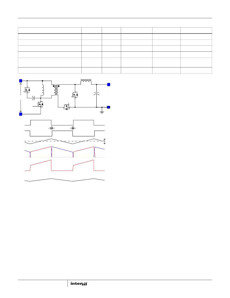
�FIGURE� 10.� OUTPUT� TIMING� DIAGRAM� FOR� N-CHANNEL� ACTIVE�
�CLAMP�
�Overlap� phasing� results� when� a� resistor� is� connected� between�
�DELAY� and� GND.� Non-overlap� phasing� results� when� a� resistor� is�
�connected� between� DELAY� and� VREF.� The� resistor� value�
�determines� the� magnitude� of� the� delay.� The� delay� feature� may�
�be� disabled� by� connecting� DELAY� directly� to� GND� or� VREF,�
�depending� on� which� configuration� is� desired,� overlap� or�
�non-overlap.� The� non-overlap� time� in� the� overlap� mode� can� be�
�calculated� using� Equation� 5.�
�the� load.� If� the� voltage� is� very� low� due� to� a� shorted� output,� large�
�currents� can� result.�
�Some� controllers� solve� the� problem� by� allowing� the� converter� to�
�cycle� on� and� off� (hic-cup� operation)� to� lower� the� average� short�
�circuit� current.� This� works� acceptably� for� some� applications,� but�
�not� when� redundancy� or� parallel� operation� is� required.� Such�
�behavior� can� prevent� a� successful� fault� recovery� when� the� short�
�is� removed.� The� paralleled� or� redundant� units� will� not� hic-cup� in�
�unison,� and� each� will� experience� an� overload� condition� each�
�time� a� restart� is� attempted.�
�An� ideal� current� limiting� method� requires� a� constant� value�
�regardless� of� the� output� voltage,� the� so-called� “brick-wall”�
�current� limit.� The� output� current� remains� constant� from� current�
�t� DELAY� =� 1.83� --------� ?� R� DELAY� (� k� Ω� )� +� 13ns�
�ns�
�k� Ω�
�(EQ.� 5)�
�limit� inception� to� a� short� circuit.� The� ISL6726� provides� this�
�behavior� with� the� average� current� limit� function.�
�(EQ.� 6)�
�t� DELAY� =� 1.79� --------� ?� R� DELAY� (� k� Ω� )� +� 9ns�
�The� deadtime� in� non-overlapping� mode� can� be� calculated� using�
�Equation� 6.�
�ns�
�k� Ω�
�See� Figure� 3� for� typical� DELAY� gain� curves.�
�14�
�The� average� current� limit� feature� uses� a� patented� circuit� that�
�samples� the� current� feedback� signal� and� creates� a� signal�
�proportional� to� the� average� value� of� the� output� inductor� current.�
�The� signal,� analogous� to� the� voltage� feedback� signal� of� voltage�
�control� loop,� becomes� the� feedback� signal� for� the� current� error�
�amplifier� and� produces� a� current� error� signal.� The� voltage�
�feedback� and� current� feedback� share� a� common� control� node�
�FN7654.0�
�January� 31,� 2011�
�相关PDF资料 |
PDF描述 |
|---|---|
| RGM08DTAT | CONN EDGECARD 16POS R/A .156 SLD |
| 0819-94K | COIL RF 820UH MOLDED UNSHIELDED |
| ISL6742AAZA | IC REG CTRLR PWM CM/VM 16-QSOP |
| VI-J5D-EY | CONVERTER MOD DC/DC 85V 50W |
| RCM18DTAT | CONN EDGECARD 36POS R/A .156 SLD |
相关代理商/技术参数 |
参数描述 |
|---|---|
| ISL6726AAZ-T | 功能描述:IC REG CTRLR ISO PWM CM 20-QSOP RoHS:是 类别:集成电路 (IC) >> PMIC - 稳压器 - DC DC 切换控制器 系列:- 产品培训模块:Lead (SnPb) Finish for COTS Obsolescence Mitigation Program 标准包装:2,500 系列:- PWM 型:电流模式 输出数:1 频率 - 最大:275kHz 占空比:50% 电源电压:18 V ~ 110 V 降压:无 升压:无 回扫:无 反相:无 倍增器:无 除法器:无 Cuk:无 隔离:是 工作温度:-40°C ~ 85°C 封装/外壳:8-SOIC(0.154",3.90mm 宽) 包装:带卷 (TR) |
| ISL6726AAZ-T7A | 功能描述:IC REG CTRLR ISO PWM CM 20-QSOP RoHS:是 类别:集成电路 (IC) >> PMIC - 稳压器 - DC DC 切换控制器 系列:- 产品培训模块:Lead (SnPb) Finish for COTS Obsolescence Mitigation Program 标准包装:2,500 系列:- PWM 型:电流模式 输出数:1 频率 - 最大:275kHz 占空比:50% 电源电压:18 V ~ 110 V 降压:无 升压:无 回扫:无 反相:无 倍增器:无 除法器:无 Cuk:无 隔离:是 工作温度:-40°C ~ 85°C 封装/外壳:8-SOIC(0.154",3.90mm 宽) 包装:带卷 (TR) |
| ISL6726EVAL1Z | 制造商:Intersil Corporation 功能描述:ISL6726 EVALUATION BOARD 1 - 20 LD QSOP - ROHS COMPLIAN - Bulk 制造商:Intersil Corporation 功能描述:BOARD EVAL FOR ISL6726 制造商:Intersil Corporation 功能描述:ISL6726 EVALUATION BOARD 1 - 20 Ld QSOP - ROHS COMPLIAN |
| ISL6729IB | 功能描述:IC REG CTRLR BST FLYBK ISO 8SOIC RoHS:否 类别:集成电路 (IC) >> PMIC - 稳压器 - DC DC 切换控制器 系列:- 标准包装:2,500 系列:- PWM 型:电流模式 输出数:1 频率 - 最大:500kHz 占空比:100% 电源电压:8.2 V ~ 30 V 降压:无 升压:无 回扫:是 反相:无 倍增器:无 除法器:无 Cuk:无 隔离:是 工作温度:0°C ~ 70°C 封装/外壳:8-DIP(0.300",7.62mm) 包装:管件 产品目录页面:1316 (CN2011-ZH PDF) |
| ISL6729IB-T | 功能描述:IC REG CTRLR BST FLYBK ISO 8SOIC RoHS:否 类别:集成电路 (IC) >> PMIC - 稳压器 - DC DC 切换控制器 系列:- 标准包装:2,500 系列:- PWM 型:电流模式 输出数:1 频率 - 最大:500kHz 占空比:100% 电源电压:8.2 V ~ 30 V 降压:无 升压:无 回扫:是 反相:无 倍增器:无 除法器:无 Cuk:无 隔离:是 工作温度:0°C ~ 70°C 封装/外壳:8-DIP(0.300",7.62mm) 包装:管件 产品目录页面:1316 (CN2011-ZH PDF) |
发布紧急采购,3分钟左右您将得到回复。