- 您现在的位置:买卖IC网 > PDF目录15216 > ISL8105AIRZ-T (Intersil)IC REG CTRLR BUCK PWM VM 10-DFN PDF资料下载
参数资料
| 型号: | ISL8105AIRZ-T |
| 厂商: | Intersil |
| 文件页数: | 14/16页 |
| 文件大小: | 0K |
| 描述: | IC REG CTRLR BUCK PWM VM 10-DFN |
| 标准包装: | 6,000 |
| PWM 型: | 电压模式 |
| 输出数: | 1 |
| 频率 - 最大: | 660kHz |
| 占空比: | 100% |
| 电源电压: | 6.5 V ~ 14.4 V |
| 降压: | 是 |
| 升压: | 无 |
| 回扫: | 无 |
| 反相: | 无 |
| 倍增器: | 无 |
| 除法器: | 无 |
| Cuk: | 无 |
| 隔离: | 无 |
| 工作温度: | -40°C ~ 85°C |
| 封装/外壳: | 10-VFDFN 裸露焊盘 |
| 包装: | 带卷 (TR) |
�� �
�
�ISL8105,� ISL8105A�
�components:� conduction� loss� and� switching� loss.� The�
�conduction� losses� are� the� largest� component� of� power�
�dissipation� for� both� the� top� and� the� bottom-side� MOSFETs.�
�These� losses� are� distributed� between� the� two� MOSFETs�
�according� to� duty� factor.� The� switching� losses� seen� when�
�sourcing� current� will� be� different� from� the� switching� losses�
�seen� when� sinking� current.� When� sourcing� current,� the�
�top-side� MOSFET� realizes� most� of� the� switching� losses.� The�
�bottom-side� switch� realizes� most� of� the� switching� losses�
�when� the� converter� is� sinking� current� (see� Equation� 14).�
�These� equations� assume� linear� voltage� current� transitions�
�and� do� not� adequately� model� power� loss� due� to� the� reverse�
�recovery� of� the� upper� and� lower� MOSFET’s� body� diode.� The�
�gate-charge� losses� are� dissipated� by� the� ISL8105� and� do� not�
�complementary� MOSFET� is� turned� on.� Also� avoid� MOSFETs�
�with� excessive� switching� times;� the� circuitry� is� expecting�
�transitions� to� occur� in� under� 50ns� or� so.�
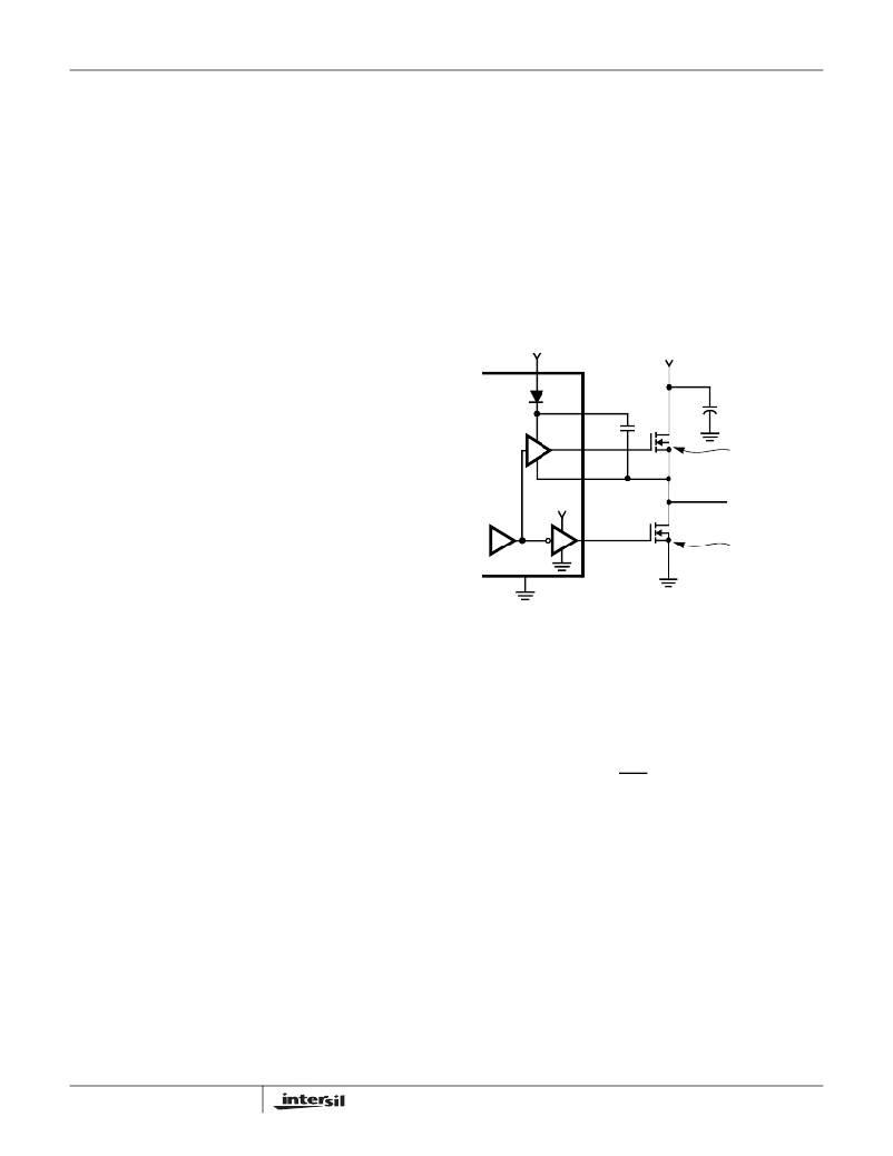
�Bootstrap� Considerations�
�Figure� 12� shows� the� top-side� gate� drive� (BOOT� pin)� supplied�
�by� a� bootstrap� circuit� from� V� BIAS� .� The� boot� capacitor,�
�C� BOOT� ,� develops� a� floating� supply� voltage� referenced� to� the�
�LX� pin.� The� supply� is� refreshed� to� a� voltage� of� V� BIAS� less�
�the� boot� diode� drop� (V� D� )� each� time� the� lower� MOSFET,� Q� 2� ,�
�turns� on.� Check� that� the� voltage� rating� of� the� capacitor� is�
�above� the� maximum� V� BIAS� voltage� in� the� system.� A� 16V�
�rating� should� be� sufficient� for� a� 12V� system.� A� value� of� 0.1μF�
�is� typical� for� many� systems� driving� single� MOSFETs.�
�heat� the� MOSFETs.� However,� large� gate� charge� increases�
�the� switching� interval,� t� SW� ,� which� increases� the� MOSFET�
�switching� losses.� Ensure� that� both� MOSFETs� are� within� their�
�maximum� junction� temperature� at� high� ambient� temperature�
�by� calculating� the� temperature� rise� according� to� package�
�+V� BIAS�
�+�
�V� D�
�-�
�BOOT�
�+1V� TO� +12V�
�thermal-resistance� specifications.� A� separate� heatsink� may�
�be� necessary� depending� upon� MOSFET� power,� package�
�type,� ambient� temperature� and� air� flow.�
�ISL8105�
�TGATE�
�C� BOOT�
�Q1�
�V� G-S� ≈� V� BIAS� -� V� D�
�LX�
�Losses� while� Sourcing� Current�
�P� TOP� =� Io� � r� DS� (� ON� )� � D� +� ---� ?� Io� � V� IN� � t� SW� � f� S�
�2� 1�
�2�
�+V� BIAS�
�P� BOTTOM� =� Io� 2� x� r� DS(ON)� x� (1� -� D)�
�Losses� while� Sinking� Current�
�-�
�+�
�BGATE�
�Q2�
�NOTE:�
�V� G-S� ≈� V� BIAS�
�P� TOP� =� Io� 2� x� r� DS(ON)� x� D�
�P� BOTTOM� =� Io� ×� r� DS� (� ON� )� ×� (� 1� –� D� )� +� ---� ?� Io� ×� V� IN� ×� t� SW� ×� f� S�
�2� 1�
�2�
�(EQ.� 14)�
�Where:�
�D� is� the� duty� cycle� =� V� OUT� /� V� IN� ,�
�t� SW� is� the� combined� switch� ON� and� OFF� time,� and�
�f� S� is� the� switching� frequency.�
�When� operating� with� a� 12V� power� supply� for� V� BIAS� (or� down�
�to� a� minimum� supply� voltage� of� 6.5V),� a� wide� variety� of�
�NMOSFETs� can� be� used.� Check� the� absolute� maximum�
�V� GS� rating� for� both� MOSFETs;� it� needs� to� be� above� the�
�highest� V� BIAS� voltage� allowed� in� the� system;� that� usually�
�means� a� 20V� V� GS� rating� (which� typically� correlates� with� a�
�30V� V� DS� maximum� rating).� Low� threshold� transistors�
�(around� 1V� or� below)� are� not� recommended� for� the� reasons�
�explained� in� the� next� paragraph.�
�For� 5V-only� operation,� given� the� reduced� available� gate� bias�
�voltage� (5V),� logic-level� transistors� should� be� used� for� both�
�N-MOSFETs.� Look� for� r� DS(ON)� ratings� at� 4.5V.� Caution�
�should� be� exercised� with� devices� exhibiting� very� low�
�V� GS(ON)� characteristics.� The� shoot-through� protection�
�present� aboard� the� ISL8105� may� be� circumvented� by� these�
�MOSFETs� if� they� have� large� parasitic� impedances� and/or�
�capacitances� that� would� inhibit� the� gate� of� the� MOSFET� from�
�being� discharged� below� its� threshold� level� before� the�
�14�
�GND�
�FIGURE� 12.� UPPER� GATE� DRIVE� -� BOOTSTRAP� OPTION�
�If� V� BIAS� is� 12V,� but� V� IN� is� lower� (such� as� 5V),� then� another�
�option� is� to� connect� the� BOOT� pin� to� 12V� and� remove� the�
�BOOT� capacitor� (although,� you� may� want� to� add� a� local�
�capacitor� from� BOOT� to� GND).� This� will� make� the� TGATE�
�V� GS� voltage� equal� to� (12V� -� 5V� =� 7V).� That� should� be� high�
�enough� to� drive� most� MOSFETs,� and� low� enough� to� improve�
�the� efficiency� slightly.� Do� NOT� leave� the� BOOT� pin� open,�
�and� try� to� get� the� same� effect� by� driving� BOOT� through�
�V� BIAS� and� the� internal� diode;� this� path� is� not� designed� for�
�the� high� current� pulses� that� will� result.�
�For� low� V� BIAS� voltage� applications� where� efficiency� is� very�
�important,� an� external� BOOT� diode� (in� parallel� with� the�
�internal� one)� may� be� considered.� The� external� diode� drop�
�has� to� be� lower� than� the� internal� one.� The� resulting� higher�
�V� G-S� of� the� top-side� FET� will� lower� its� r� DS(ON)� .� The� modest�
�gain� in� efficiency� should� be� balanced� against� the� extra� cost�
�and� area� of� the� external� diode.�
�For� information� on� the� Application� circuit,� including� a�
�complete� Bill-of-Materials� and� circuit� board� description,� can�
�be� found� in� Application� Note� AN1258.�
�http://www.intersil.com/data/an/AN1258.pdf�
�FN6306.5�
�April� 15,� 2010�
�相关PDF资料 |
PDF描述 |
|---|---|
| ISL8105BIRZ-T | IC REG CTRLR BUCK PWM VM 10-DFN |
| B41041A6108M | 1000UF 50V 16X25 SINGLE END |
| ISL8105IRZ-T | IC REG CTRLR BUCK PWM VM 10-DFN |
| MC33164DM-3R2G | IC SENSOR UNDERVOLTAGE 8-MICRO |
| RBM28DSXH | CONN EDGECARD 56POS DIP .156 SLD |
相关代理商/技术参数 |
参数描述 |
|---|---|
| ISL8105B | 制造商:INTERSIL 制造商全称:Intersil Corporation 功能描述:+5V or +12V Single-Phase Synchronous Buck Converter PWM Controller with Integrated MOSFET Gate Drivers, Extended Soft-Start Time |
| ISL8105BCBZ | 功能描述:IC REG CTRLR BUCK PWM VM 8-SOIC RoHS:是 类别:集成电路 (IC) >> PMIC - 稳压器 - DC DC 切换控制器 系列:- 产品培训模块:Lead (SnPb) Finish for COTS Obsolescence Mitigation Program 标准包装:2,500 系列:- PWM 型:电流模式 输出数:1 频率 - 最大:275kHz 占空比:50% 电源电压:18 V ~ 110 V 降压:无 升压:无 回扫:无 反相:无 倍增器:无 除法器:无 Cuk:无 隔离:是 工作温度:-40°C ~ 85°C 封装/外壳:8-SOIC(0.154",3.90mm 宽) 包装:带卷 (TR) |
| ISL8105BCBZ-T | 功能描述:IC REG CTRLR BUCK PWM VM 8-SOIC RoHS:是 类别:集成电路 (IC) >> PMIC - 稳压器 - DC DC 切换控制器 系列:- 标准包装:4,500 系列:PowerWise® PWM 型:控制器 输出数:1 频率 - 最大:1MHz 占空比:95% 电源电压:2.8 V ~ 5.5 V 降压:是 升压:无 回扫:无 反相:无 倍增器:无 除法器:无 Cuk:无 隔离:无 工作温度:-40°C ~ 125°C 封装/外壳:6-WDFN 裸露焊盘 包装:带卷 (TR) 配用:LM1771EVAL-ND - BOARD EVALUATION LM1771 其它名称:LM1771SSDX |
| ISL8105BCRZ | 功能描述:IC REG CTRLR BUCK PWM VM 10-DFN RoHS:是 类别:集成电路 (IC) >> PMIC - 稳压器 - DC DC 切换控制器 系列:- 产品培训模块:Lead (SnPb) Finish for COTS Obsolescence Mitigation Program 标准包装:2,500 系列:- PWM 型:电流模式 输出数:1 频率 - 最大:275kHz 占空比:50% 电源电压:18 V ~ 110 V 降压:无 升压:无 回扫:无 反相:无 倍增器:无 除法器:无 Cuk:无 隔离:是 工作温度:-40°C ~ 85°C 封装/外壳:8-SOIC(0.154",3.90mm 宽) 包装:带卷 (TR) |
| ISL8105BCRZ-T | 功能描述:IC REG CTRLR BUCK PWM VM 10-DFN RoHS:是 类别:集成电路 (IC) >> PMIC - 稳压器 - DC DC 切换控制器 系列:- 标准包装:4,500 系列:PowerWise® PWM 型:控制器 输出数:1 频率 - 最大:1MHz 占空比:95% 电源电压:2.8 V ~ 5.5 V 降压:是 升压:无 回扫:无 反相:无 倍增器:无 除法器:无 Cuk:无 隔离:无 工作温度:-40°C ~ 125°C 封装/外壳:6-WDFN 裸露焊盘 包装:带卷 (TR) 配用:LM1771EVAL-ND - BOARD EVALUATION LM1771 其它名称:LM1771SSDX |
发布紧急采购,3分钟左右您将得到回复。