- 您现在的位置:买卖IC网 > PDF目录15524 > ISL8130IRZ (Intersil)IC REG CTRLR BST FLYBK PWM 20QFN PDF资料下载
参数资料
| 型号: | ISL8130IRZ |
| 厂商: | Intersil |
| 文件页数: | 16/24页 |
| 文件大小: | 0K |
| 描述: | IC REG CTRLR BST FLYBK PWM 20QFN |
| 标准包装: | 75 |
| PWM 型: | 电压模式 |
| 输出数: | 1 |
| 频率 - 最大: | 1.4MHz |
| 占空比: | 100% |
| 电源电压: | 4.5 V ~ 5.5 V |
| 降压: | 是 |
| 升压: | 是 |
| 回扫: | 是 |
| 反相: | 无 |
| 倍增器: | 无 |
| 除法器: | 无 |
| Cuk: | 无 |
| 隔离: | 无 |
| 工作温度: | -40°C ~ 85°C |
| 封装/外壳: | 20-VFQFN 裸露焊盘 |
| 包装: | 管件 |
�� �
�
�ISL8130�
�threshold.� A� Kelvin� connection� is� recommended� to� avoid� noise�
�coupling.�
�In� a� buck� configuration,� the� OC� trip� point� varies� mainly� due� to� the�
�upper� MOSFETs� r� DS(ON)� variations.� To� avoid� overcurrent� tripping� in�
�the� normal� operating� load� range,� find� the� R� OCSET� resistor� from�
�Equation� 1� with:�
�1.� The� maximum� r� DS(ON)� at� the� highest� junction� temperature.�
�2.� Determine� I� OC� for� I� OC� >� I� OUT� (� MAX� )� +� (� Δ� I� )� ?� 2� ,�
�where� Δ� I� is� the� output� inductor� ripple� current.�
�A� small� ceramic� capacitor� should� be� placed� in� parallel� with�
�R� OCSET� to� smooth� the� voltage� across� R� OCSET� in� the� presence� of�
�switching� noise� on� the� input� voltage.� Both� the� R� OCSET� and� the�
�filtering� cap� should� be� placed� close� to� the� ISL8130.�
�The� OCP� function� is� active� once� the� ENSs� reaches� the� enable�
�threshold� voltage.�
�Over-Temperature� Protection�
�The� ISL8130� is� protected� against� over-temperature� conditions.�
�When� the� junction� temperature� exceeds� +150°C,� the� PWM� shuts�
�off.� Normal� operation� is� resumed� when� the� junction� temperature�
�decreases� to� 130°C.�
�Undervoltage�
�If� the� voltage� on� the� FB� pin� is� less� than� 85%� of� the� reference�
�voltage� for� 8� consecutive� PWM� cycles,� then� the� circuit� enters� into�
�Application� Guidelines�
�Layout� Considerations�
�As� in� any� high� frequency� switching� converter,� layout� is� very�
�important.� Switching� current� from� one� power� device� to� another�
�can� generate� voltage� transients� across� the� impedances� of� the�
�interconnecting� bond� wires� and� circuit� traces.� These�
�interconnecting� impedances� should� be� minimized� by� using� wide,�
�short� printed� circuit� traces.� The� critical� components� should� be�
�located� as� close� together� as� possible� using� ground� plane�
�construction� or� single� point� grounding.�
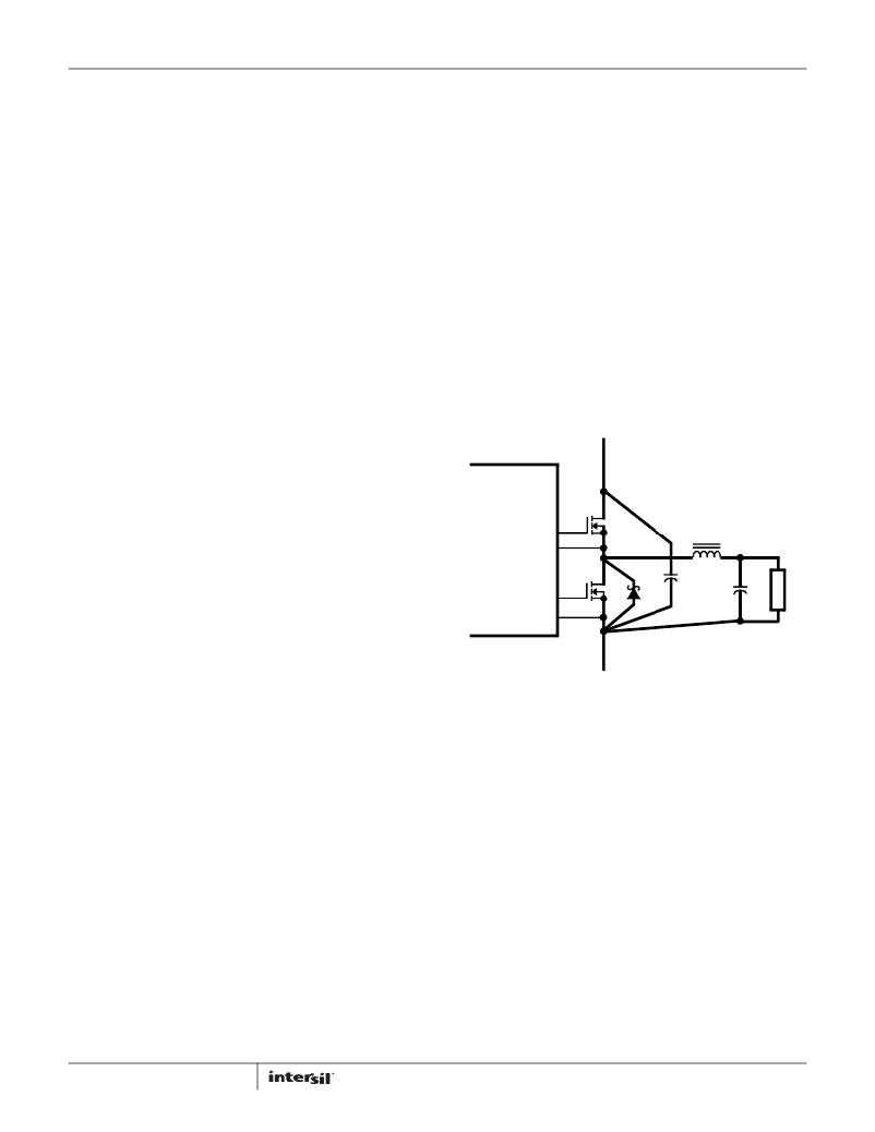
�Figure� 29� shows� the� critical� power� components� of� the� buck�
�converter.� To� minimize� the� voltage� overshoot� the� interconnecting�
�wires� indicated� by� heavy� lines� should� be� part� of� ground� or� power�
�plane� in� a� printed� circuit� board.� The� components� shown� in�
�Figure� 29� should� be� located� as� close� together� as� possible.� Please�
�note� that� the� capacitors� C� IN� and� C� O� each� represent� numerous�
�physical� capacitors.� Locate� the� ISL8130� within� 3� inches� of� the�
�MOSFETs,� Q� 1� and� Q� 2� .� The� circuit� traces� for� the� MOSFETs’� gate�
�and� source� connections� from� the� ISL8130� must� be� sized� to�
�handle� up� to� 1A� peak� current.�
�VIN�
�ISL8130�
�soft-start� hiccup� mode.� This� mode� is� identical� to� the� overcurrent�
�hiccup� mode.� This� undervoltage� protection� is� disabled� if� the�
�ENSS� does� not� reach� 3.3V.�
�UGATE�
�PHASE�
�Q1�
�L� O�
�V� OUT�
�Overvoltage� Protection�
�If� the� voltage� on� the� FB� pin� exceeds� the� reference� voltage� by� 15%,�
�LGATE�
�Q2�
�D2�
�C� IN�
�C� O�
�the� lower� gate� driver� is� turned� on� continuously� to� discharge� the�
�output� voltage.� If� the� overvoltage� condition� continues� for� 32�
�consecutive� PWM� cycles,� then� the� chip� is� turned� off� with� the� gate�
�drivers� tri-stated.� The� voltage� on� the� FB� pin� will� fall� and� reach� the�
�15%� undervoltage� threshold.� After� 8� clock� cycles,� the� chip� will�
�enter� soft-start� hiccup� mode.� This� mode� is� identical� to� the�
�overcurrent� hiccup� mode.� This� overvoltage� protection� is� disabled�
�if� the� ENSS� does� not� reach� 3.3V.�
�Gate� Control� Logic�
�The� gate� control� logic� translates� PWM� control� signals� into� the�
�MOSFET� gate� drive� signals� providing� necessary� amplification,�
�level� shifting� and� shoot-through� protection.� Also,� it� has� functions�
�that� help� optimize� the� IC� performance� over� a� wide� range� of�
�operational� conditions.�
�Since� MOSFET� switching� time� can� vary� dramatically� from� type� to�
�type� and� with� the� input� voltage,� the� gate� control� logic� provides�
�adaptive� dead� time� by� monitoring� the� gate-to-source� voltages� of�
�both� upper� and� lower� MOSFETs.� The� lower� MOSFET� is� not� turned�
�on� until� the� gate-to-source� voltage� of� the� upper� MOSFET� has�
�decreased� to� less� than� approximately� 1V.� Similarly,� the� upper�
�MOSFET� is� not� turned� on� until� the� gate-to-source� voltage� of� the�
�lower� MOSFET� has� decreased� to� less� than� approximately� 1V.� This�
�allows� a� wide� variety� of� upper� and� lower� MOSFETs� to� be� used�
�without� a� concern� for� simultaneous� conduction,� or� shoot-through.�
�In� a� boost� converter� configuration,� the� LGATE� signal� may� be� left�
�floating.�
�16�
�GND�
�RETURN�
�FIGURE� 29.� PRINTED� CIRCUIT� BOARD� POWER� AND� GROUND�
�PLANES� OR� ISLANDS�
�Figure� 30� shows� the� circuit� traces� that� require� additional� layout�
�consideration.� Use� single� point� and� ground� plane� construction� for�
�the� circuits� shown.� Minimize� any� leakage� current� paths� on� the� SS�
�PIN� and� locate� the� capacitor,� C� ss� close� to� the� SS� pin� because� the�
�internal� current� source� is� only� 10μA.� Provide� local� V� CC�
�decoupling� between� VCC� and� GND� pins.� Locate� the� capacitor,�
�C� BOOT� as� close� as� practical� to� the� BOOT� and� PHASE� pins.�
�FN7954.3�
�October� 5,� 2012�
�相关PDF资料 |
PDF描述 |
|---|---|
| ADZS-BF537-ASKIT | BOARD EVAL SKIT ADSP-BF537 |
| ECC18DRAS | CONN EDGECARD 36POS R/A .100 SLD |
| V300C36C75BF | CONVERTER MOD DC/DC 36V 75W |
| SEK100M250ST | CAP ALUM 10UF 250V 20% RADIAL |
| AT91SAM9260-EK | KIT EVAL FOR AT91SAM9260 |
相关代理商/技术参数 |
参数描述 |
|---|---|
| ISL8130IRZ-T7A | 功能描述:电流型 PWM 控制器 Pb-Free W/Anneal SYNC BUCK PWM CONT. WITH 4.5V-28V INPUT,20 RoHS:否 制造商:Texas Instruments 开关频率:27 KHz 上升时间: 下降时间: 工作电源电压:6 V to 15 V 工作电源电流:1.5 mA 输出端数量:1 最大工作温度:+ 105 C 安装风格:SMD/SMT 封装 / 箱体:TSSOP-14 |
| ISL8130IRZ-TK | 功能描述:IC REG CTRLR BST FLYBK PWM 20QFN RoHS:是 类别:集成电路 (IC) >> PMIC - 稳压器 - DC DC 切换控制器 系列:- 产品培训模块:Lead (SnPb) Finish for COTS Obsolescence Mitigation Program 标准包装:2,500 系列:- PWM 型:电流模式 输出数:1 频率 - 最大:275kHz 占空比:50% 电源电压:18 V ~ 110 V 降压:无 升压:无 回扫:无 反相:无 倍增器:无 除法器:无 Cuk:无 隔离:是 工作温度:-40°C ~ 85°C 封装/外壳:8-SOIC(0.154",3.90mm 宽) 包装:带卷 (TR) |
| ISL81334 | 制造商:INTERSIL 制造商全称:Intersil Corporation 功能描述:【15kV ESD Protected, 5V, Two Port, Dual Protocol (RS-232/RS-485) Transceivers |
| ISL81334_07 | 制造商:INTERSIL 制造商全称:Intersil Corporation 功能描述:【15kV ESD Protected, 5V, Two Port, Dual Protocol (RS-232/RS-485) Transceivers |
| ISL81334IAZ | 功能描述:IC TXRX DUAL 2PORT ESD 28-SSOP RoHS:是 类别:集成电路 (IC) >> 接口 - 驱动器,接收器,收发器 系列:- 产品培训模块:Lead (SnPb) Finish for COTS Obsolescence Mitigation Program 标准包装:50 系列:- 类型:收发器 驱动器/接收器数:1/1 规程:RS422,RS485 电源电压:4.75 V ~ 5.25 V 安装类型:通孔 封装/外壳:8-DIP(0.300",7.62mm) 供应商设备封装:8-PDIP 包装:管件 产品目录页面:1402 (CN2011-ZH PDF) |
发布紧急采购,3分钟左右您将得到回复。