- 您现在的位置:买卖IC网 > PDF目录15524 > ISL8130IRZ (Intersil)IC REG CTRLR BST FLYBK PWM 20QFN PDF资料下载
参数资料
| 型号: | ISL8130IRZ |
| 厂商: | Intersil |
| 文件页数: | 18/24页 |
| 文件大小: | 0K |
| 描述: | IC REG CTRLR BST FLYBK PWM 20QFN |
| 标准包装: | 75 |
| PWM 型: | 电压模式 |
| 输出数: | 1 |
| 频率 - 最大: | 1.4MHz |
| 占空比: | 100% |
| 电源电压: | 4.5 V ~ 5.5 V |
| 降压: | 是 |
| 升压: | 是 |
| 回扫: | 是 |
| 反相: | 无 |
| 倍增器: | 无 |
| 除法器: | 无 |
| Cuk: | 无 |
| 隔离: | 无 |
| 工作温度: | -40°C ~ 85°C |
| 封装/外壳: | 20-VFQFN 裸露焊盘 |
| 包装: | 管件 |
�� �
�
�ISL8130�
�Compensation� Break� Frequency� Equations�
�Component� Selection� Guidelines�
�F� Z1� =� ----------------------------------�
�F� P1� =� -------------------------------------------------------�
�2� π� ?� R2� ?� ?� ----------------------� ?�
�F� Z2� =� ------------------------------------------------------�
�F� P2� =� ----------------------------------�
�1�
�2� π� ?� R� 2� ?� C1�
�1�
�C1� ?� C2�
�?� C1� +� C2� ?�
�1�
�2� π� ?� (� R1� +� R3� )� ?� C3�
�1�
�2� π� ?� R3� ?� C3�
�(EQ.� 6)�
�(EQ.� 7)�
�(EQ.� 8)�
�(EQ.� 9)�
�Buck� Converter� Component�
�MOSFET� CONSIDERATIONS�
�The� logic� level� MOSFETs� are� chosen� for� optimum� efficiency� given�
�the� potentially� wide� input� voltage� range� and� output� power�
�requirements,� two� N-Channel� MOSFETs� for� the� Buck� converter.�
�These� MOSFETs� should� be� selected� based� upon� r� DS(ON)� ,� gate�
�supply� requirements,� and� thermal� management� considerations.�
�The� power� dissipation� includes� two� loss� components;� conduction�
�(� I� O� )� (� r� DS� (� ON� )� )� (� V� OUT� )�
�(� I� O� )� (� V� IN� )� (� t� SW� )� (� F� SW� )�
�P� UPPER� =� ---------------------------------------------------------------� +� ------------------------------------------------------------�
�V� IN�
�1.� Pick� Gain� (R2/R1)� for� desired� converter� bandwidth�
�2.� Place� 1� ST� Zero� Below� Filter’s� Double� Pole� (~75%� F� LC� )�
�3.� Place� 2� ND� Zero� at� Filter’s� Double� Pole�
�4.� Place� 1� ST� Pole� at� the� ESR� Zero�
�5.� Place� 2� ND� Pole� at� Half� the� Switching� Frequency�
�6.� Check� Gain� against� Error� Amplifier’s� Open-Loop� Gain�
�7.� Estimate� Phase� Margin� -� Repeat� if� Necessary�
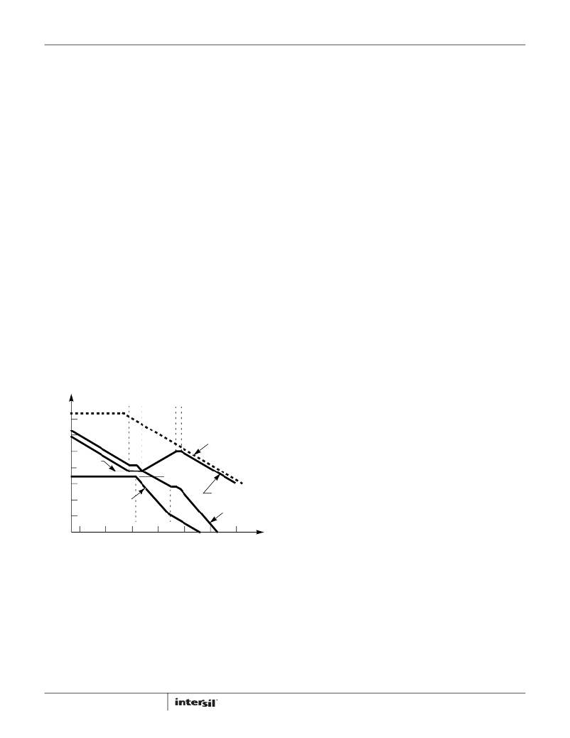
�Figure� 33� shows� an� asymptotic� plot� of� the� DC/DC� converter’s� gain�
�vs� frequency.� The� actual� Modulator� Gain� has� a� high� gain� peak� due�
�to� the� high� Q� factor� of� the� output� filter� and� is� not� shown� in�
�Figure� 33.� Using� the� previously� mentioned� guidelines� should� give�
�a� compensation� gain� similar� to� the� curve� plotted.� The� open� loop�
�loss� and� switching� loss.� These� losses� are� distributed� between� the�
�upper� and� lower� MOSFETs� according� to� duty� cycle� (see�
�Equations� 10� and� 11).� The� conduction� losses� are� the� main�
�component� of� power� dissipation� for� the� lower� MOSFETs.� Only� the�
�upper� MOSFET� has� significant� switching� losses� since� the� lower�
�device� turns� on� and� off� into� near� zero� voltage.� The� equations�
�assume� linear� voltage-current� transitions� and� do� not� model�
�power� loss� due� to� the� reverse-recovery� of� the� lower� MOSFET’s�
�body� diode.�
�2�
�2�
�(EQ.� 10)�
�(� I� O� )� (� r� DS� (� ON� )� )� (� V� IN� –� V� OUT� )�
�P� LOWER� =� -------------------------------------------------------------------------------�
�error� amplifier� gain� bounds� the� compensation� gain.� Check� the�
�compensation� gain� at� F� P2� with� the� capabilities� of� the� error�
�amplifier.� The� Loop� Gain� is� constructed� on� the� log-log� graph� of�
�2�
�V� IN�
�(EQ.� 11)�
�Figure� 33� by� adding� the� Modulator� Gain� (in� dB)� to� the�
�Compensation� Gain� (in� dB).� This� is� equivalent� to� multiplying� the�
�modulator� transfer� function� to� the� compensation� transfer� function�
�and� plotting� the� gain.�
�A� large� gate-charge� increases� the� switching� time,� t� SW� ,� which�
�increases� the� upper� MOSFET� switching� losses.� Ensure� that� both�
�MOSFETs� are� within� their� maximum� junction� temperature� at� high�
�ambient� temperature� by� calculating� the� temperature� rise� according�
�100�
�80�
�60�
�F� Z� 1� F� Z2�
�F� P1�
�F� P2�
�OPEN� LOOP�
�ERROR� AMP� GAIN�
�to� package� thermal-resistance� specifications.�
�OUTPUT� INDUCTOR� SELECTION�
�The� PWM� converters� require� output� inductors.� The� output�
�inductor� is� selected� to� meet� the� output� voltage� ripple�
�-40�
�F� ESR�
�Δ� I� L� =� ----------------------------------------------------------�
�(� V� IN� –� V� OUT� )� (� V� OUT� )�
�(� f� S� )� (� L� )� (� V� IN� )�
�40�
�20LOG�
�20� (R� 2� /R� 1� )� 20LOG�
�(VIN/DV� OSC� )�
�0�
�COMPENSATION�
�-20� MODULATOR� GAIN�
�GAIN�
�LOOP� GAIN�
�F� LC�
�-60�
�10� 100� 1k� 10k� 100k� 1M� 10M�
�FREQUENCY� (Hz)�
�FIGURE� 33.� ASYMPTOTIC� BODE� PLOT� OF� CONVERTER� GAIN�
�The� compensation� gain� uses� external� impedance� networks� Z� FB�
�and� Z� IN� to� provide� a� stable,� high� bandwidth� (BW)� overall� loop.� A�
�stable� control� loop� has� a� gain� crossing� with� -20dB/decade� slope�
�and� a� phase� margin� greater� than� 45°.� Include� worst� case�
�component� variations� when� determining� phase� margin.�
�18�
�requirements.� The� inductor� value� determines� the� converter’s�
�ripple� current� and� the� ripple� voltage� is� a� function� of� the� ripple�
�current� and� output� capacitor(s)� ESR.� The� ripple� voltage�
�expression� is� given� in� the� capacitor� selection� section� and� the�
�ripple� current� is� approximated� by� Equation� 12:�
�(EQ.� 12)�
�OUTPUT� CAPACITOR� SELECTION�
�The� output� capacitors� should� be� selected� to� meet� the� dynamic�
�regulation� requirements� including� ripple� voltage� and� load�
�transients.� Selection� of� output� capacitors� is� also� dependent� on�
�the� output� inductor,� thus� some� inductor� analysis� is� required� to�
�select� the� output� capacitors.�
�One� of� the� parameters� limiting� the� converter’s� response� to� a� load�
�transient� is� the� time� required� for� the� inductor� current� to� slew� to�
�its� new� level.� The� response� time� is� the� time� interval� required� to�
�slew� the� inductor� current� from� an� initial� current� value� to� the� load�
�current� level.� During� this� interval� the� difference� between� the�
�inductor� current� and� the� transient� current� level� must� be� supplied�
�by� the� output� capacitor(s).� Minimizing� the� response� time� can�
�FN7954.3�
�October� 5,� 2012�
�相关PDF资料 |
PDF描述 |
|---|---|
| ADZS-BF537-ASKIT | BOARD EVAL SKIT ADSP-BF537 |
| ECC18DRAS | CONN EDGECARD 36POS R/A .100 SLD |
| V300C36C75BF | CONVERTER MOD DC/DC 36V 75W |
| SEK100M250ST | CAP ALUM 10UF 250V 20% RADIAL |
| AT91SAM9260-EK | KIT EVAL FOR AT91SAM9260 |
相关代理商/技术参数 |
参数描述 |
|---|---|
| ISL8130IRZ-T7A | 功能描述:电流型 PWM 控制器 Pb-Free W/Anneal SYNC BUCK PWM CONT. WITH 4.5V-28V INPUT,20 RoHS:否 制造商:Texas Instruments 开关频率:27 KHz 上升时间: 下降时间: 工作电源电压:6 V to 15 V 工作电源电流:1.5 mA 输出端数量:1 最大工作温度:+ 105 C 安装风格:SMD/SMT 封装 / 箱体:TSSOP-14 |
| ISL8130IRZ-TK | 功能描述:IC REG CTRLR BST FLYBK PWM 20QFN RoHS:是 类别:集成电路 (IC) >> PMIC - 稳压器 - DC DC 切换控制器 系列:- 产品培训模块:Lead (SnPb) Finish for COTS Obsolescence Mitigation Program 标准包装:2,500 系列:- PWM 型:电流模式 输出数:1 频率 - 最大:275kHz 占空比:50% 电源电压:18 V ~ 110 V 降压:无 升压:无 回扫:无 反相:无 倍增器:无 除法器:无 Cuk:无 隔离:是 工作温度:-40°C ~ 85°C 封装/外壳:8-SOIC(0.154",3.90mm 宽) 包装:带卷 (TR) |
| ISL81334 | 制造商:INTERSIL 制造商全称:Intersil Corporation 功能描述:【15kV ESD Protected, 5V, Two Port, Dual Protocol (RS-232/RS-485) Transceivers |
| ISL81334_07 | 制造商:INTERSIL 制造商全称:Intersil Corporation 功能描述:【15kV ESD Protected, 5V, Two Port, Dual Protocol (RS-232/RS-485) Transceivers |
| ISL81334IAZ | 功能描述:IC TXRX DUAL 2PORT ESD 28-SSOP RoHS:是 类别:集成电路 (IC) >> 接口 - 驱动器,接收器,收发器 系列:- 产品培训模块:Lead (SnPb) Finish for COTS Obsolescence Mitigation Program 标准包装:50 系列:- 类型:收发器 驱动器/接收器数:1/1 规程:RS422,RS485 电源电压:4.75 V ~ 5.25 V 安装类型:通孔 封装/外壳:8-DIP(0.300",7.62mm) 供应商设备封装:8-PDIP 包装:管件 产品目录页面:1402 (CN2011-ZH PDF) |
发布紧急采购,3分钟左右您将得到回复。