- 您现在的位置:买卖IC网 > PDF目录17314 > ISL8200MEVAL1PHZ (Intersil)EVAL BAORD FOR ISL8200 PDF资料下载
参数资料
| 型号: | ISL8200MEVAL1PHZ |
| 厂商: | Intersil |
| 文件页数: | 20/23页 |
| 文件大小: | 0K |
| 描述: | EVAL BAORD FOR ISL8200 |
| 产品培训模块: | Solutions for Industrial Control Applications |
| 标准包装: | 1 |
| 主要目的: | DC/DC,步降 |
| 输出及类型: | 1,非隔离 |
| 输出电压: | 0.6 ~ 6 V |
| 电流 - 输出: | 10A |
| 输入电压: | 3 ~ 20 V |
| 稳压器拓扑结构: | 降压 |
| 频率 - 开关: | 700kHz ~ 1.5MHz |
| 板类型: | 完全填充 |
| 已供物品: | 板 |
| 已用 IC / 零件: | ISL8200 |
�� �
�
�ISL8200M�
�Thermal� Vias�
�A� grid� of� 1.0mm� to� 1.2mm� pitch� thermal� vias,� which�
�drops� down� and� connects� to� buried� copper� plane(s),�
�should� be� placed� under� the� thermal� land.� The� vias� should�
�be� about� 0.3mm� to� 0.33mm� in� diameter� with� the� barrel�
�plated� to� about� 1.0� ounce� copper.� Although� adding� more�
�vias� (by� decreasing� via� pitch)� will� improve� the� thermal�
�performance,� diminishing� returns� will� be� seen� as� more�
�and� more� vias� are� added.� Simply� use� as� many� vias� as�
�practical� for� the� thermal� land� size� and� your� board� design�
�rules� allow.�
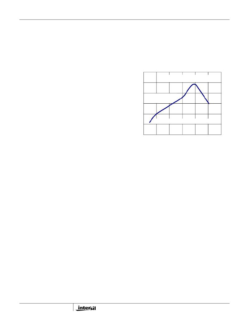
�Reflow� Parameters�
�Due� to� the� low� mount� height� of� the� QFN,� "No� Clean"� Type� 3�
�solder� paste� per� ANSI/J-STD-00� is� recommended.� Nitrogen�
�purge� is� also� recommended� during� reflow.� A� system� board�
�reflow� profile� depends� on� the� thermal� mass� of� the� entire�
�populated� board,� so� it� is� not� practical� to� define� a� specific�
�soldering� profile� just� for� the� QFN.� The� profile� given� in�
�Figure� 33� is� provided� as� a� guideline,� to� be� customized� for�
�varying� manufacturing� practices� and� applications.�
�300�
�Stencil� Pattern� Design�
�Reflowed� solder� joints� on� the� perimeter� I/O� lands� should�
�have� about� a� 50μm� to� 75μm� (2mil� to� 3mil)� standoff�
�height.� The� solder� paste� stencil� design� is� the� first� step� in�
�developing� optimized,� reliable� solder� joins.� Stencil�
�aperture� size� to� land� size� ratio� should� typically� be� 1:1.� The�
�aperture� width� may� be� reduced� slightly� to� help� prevent�
�solder� bridging� between� adjacent� I/O� lands.� To� reduce�
�solder� paste� volume� on� the� larger� thermal� lands,� it� is�
�recommended� that� an� array� of� smaller� apertures� be� used�
�instead� of� one� large� aperture.� It� is� recommended� that� the�
�stencil� printing� area� cover� 50%� to� 80%� of� the� PCB� layout�
�250�
�200�
�150�
�100�
�50�
�PEAK� TEMPERATURE� +230°C~+245°C;�
�KEEP� ABOUT� 30s� ABOVE� +220°C�
�SLOW� RAMP� AND�
�SOAK� FROM� +100°C� TO�
�+180°C� FOR� 90s~120s�
�RAMP� RATE� ≤� 1.5°C� FROM� +70°C� TO� +90°C�
�pattern.� A� typical� solder� stencil� pattern� is� shown� in� the�
�Package� Outline� Drawing� L23.15x15� on� page� 22.� The� gap�
�0�
�0�
�100�
�150�
�200�
�250�
�50�
�300�
�width� between� pad� to� pad� is� 0.6mm.� The� user� should�
�consider� the� symmetry� of� the� whole� stencil� pattern� when�
�designing� its� pads.� A� laser� cut,� stainless� steel� stencil� with�
�electropolished� trapezoidal� walls� is� recommended.�
�Electropolishing� “smooths”� the� aperture� walls� resulting� in�
�reduced� surface� friction� and� better� paste� release� which�
�reduces� voids.� Using� a� trapezoidal� section� aperture� (TSA)�
�also� promotes� paste� release� and� forms� a� "brick� like"� paste�
�deposit� that� assists� in� firm� component� placement.� A�
�0.1mm� to� 0.15mm� stencil� thickness� is� recommended� for�
�this� large� pitch� (1.3mm)� QFN.�
�20�
�DURATION� (s)�
�FIGURE� 33.� TYPICAL� REFLOW� PROFILE�
�FN6727.1�
�February� 26,� 2010�
�相关PDF资料 |
PDF描述 |
|---|---|
| ECM10DSXH | CONN EDGECARD 20POS DIP .156 SLD |
| ISL8105AEVAL1Z | EVALUATION BOARD FOR ISL8105A |
| EBM12DSES | CONN EDGECARD 24POS .156 EYELET |
| EBM10DSEI | CONN EDGECARD 20POS .156 EYELET |
| EEM15DRYS | CONN EDGECARD 30POS DIP .156 SLD |
相关代理商/技术参数 |
参数描述 |
|---|---|
| ISL8200MEVAL2PHZ | 功能描述:电源管理IC开发工具 ISL8200M EVAL BBRD 2 PHS 23LD ROH RoHS:否 制造商:Maxim Integrated 产品:Evaluation Kits 类型:Battery Management 工具用于评估:MAX17710GB 输入电压: 输出电压:1.8 V |
| ISL8200MIRZ | 功能描述:DC/DC转换器 STAND ALONE 10A DC/D CSTEPDWNPWRSUPPYMOD1 RoHS:否 制造商:Murata 产品: 输出功率: 输入电压范围:3.6 V to 5.5 V 输入电压(标称): 输出端数量:1 输出电压(通道 1):3.3 V 输出电流(通道 1):600 mA 输出电压(通道 2): 输出电流(通道 2): 安装风格:SMD/SMT 封装 / 箱体尺寸: |
| ISL8200MIRZ-T | 功能描述:DC/DC转换器 ST& ALONE 10A DC/DC DWN PWR SUPPLY MOD RoHS:否 制造商:Murata 产品: 输出功率: 输入电压范围:3.6 V to 5.5 V 输入电压(标称): 输出端数量:1 输出电压(通道 1):3.3 V 输出电流(通道 1):600 mA 输出电压(通道 2): 输出电流(通道 2): 安装风格:SMD/SMT 封装 / 箱体尺寸: |
| ISL8200MIRZ-TR5545 | 制造商:Intersil Corporation 功能描述:STAND ALONE 10A DC/DC STEP DOWN POWER SUPPLY MODULE, 15 X 15 - Tape and Reel |
| ISL8200MMREP | 制造商:Intersil Corporation 功能描述:V62/10608-01XB, STAND ALONE 10A DC/DC STEP DOWN POWER SUPPLY - Trays |
发布紧急采购,3分钟左右您将得到回复。