- 您现在的位置:买卖IC网 > Datasheet目录334 > ISL8501EVAL1Z (Intersil)EVALUATION BOARD FOR ISL8501 Datasheet资料下载
参数资料
| 型号: | ISL8501EVAL1Z |
| 厂商: | Intersil |
| 文件页数: | 18/19页 |
| 文件大小: | 0K |
| 描述: | EVALUATION BOARD FOR ISL8501 |
| 标准包装: | 1 |
| 主要目的: | DC/DC,LDO 步降 |
| 输出及类型: | 3,非隔离 |
| 输出电压: | 3.3V,1.2V,1.8V |
| 电流 - 输出: | 1A,500mA,500mA |
| 输入电压: | 4.5 ~ 25 V |
| 稳压器拓扑结构: | 降压 |
| 频率 - 开关: | 500kHz |
| 板类型: | 完全填充 |
| 已供物品: | 板 |
| 已用 IC / 零件: | ISL8501 |
�� �
�
�ISL8501�
�The� compensation� gain� uses� external� impedance� networks�
�Z� FB� and� Z� IN� to� provide� a� stable,� high� bandwidth� (BW)� overall�
�loop.� A� stable� control� loop� has� a� gain� crossing� with�
�-20dB/decade� slope� and� a� phase� margin� greater� than� 45°.�
�Include� worst� case� component� variations� when� determining�
�phase� margin.�
�A� more� detailed� explanation� of� voltage� mode� control� of� a�
�buck� regulator� can� be� found� in� Tech� Brief� TB417,� titled�
�“Designing� Stable� Compensation� Networks� for� Single� Phase�
�Voltage� Mode� Buck� Regulators.”�
�represent� numerous� physical� capacitors.� Dedicate� one� solid�
�layer� (usually� a� middle� layer� of� the� PC� board)� for� a� ground�
�plane� and� make� all� critical� component� ground� connections�
�with� vias� to� this� layer.� Dedicate� another� solid� layer� as� a�
�power� plane� and� break� this� plane� into� smaller� islands� of�
�common� voltage� levels.� Keep� the� metal� runs� from� the�
�PHASE� terminals� to� the� output� inductor� short.� The� power�
�plane� should� support� the� input� power� and� output� power�
�nodes.� Use� copper� filled� polygons� on� the� top� and� bottom�
�circuit� layers� for� the� phase� nodes.� Use� the� remaining� printed�
�circuit� layers� for� small� signal� wiring.�
�100�
�f� Z1� f� Z2�
�f� P1�
�f� P2�
�In� order� to� dissipate� heat� generated� by� the� internal� LDO� and�
�80�
�MOSFET,� the� ground� pad,� pin� 29,� should� be� connected� to�
�60�
�40�
�20LOG�
�OPEN� LOOP�
�ERROR� AMP� GAIN�
�the� internal� ground� plane� through� at� least� four� vias.� This�
�allows� the� heat� to� move� away� from� the� IC� and� also� ties� the�
�pad� to� the� ground� plane� through� a� low� impedance� path.�
�20�
�0�
�(R� 2� /R� 1� )�
�20LOG�
�(V� IN� /� Δ� V� OSC� )�
�The� switching� components� should� be� placed� close� to� the�
�ISL8501� first.� Minimize� the� length� of� the� connections�
�-20�
�-40�
�-60�
�MODULATOR�
�GAIN�
�f� LC�
�f� ESR�
�COMPENSATION�
�GAIN�
�CLOSED� LOOP�
�GAIN�
�between� the� input� capacitors,� C� IN� ,� and� the� power� switches�
�by� placing� them� nearby.� Position� both� the� ceramic� and� bulk�
�input� capacitors� as� close� to� the� upper� MOSFET� drain� as�
�possible.� Position� the� output� inductor� and� output� capacitors�
�10�
�100�
�1k�
�10k�
�100k�
�1M�
�10M�
�between� the� upper� and� lower� MOSFETs� and� the� load.�
�FREQUENCY� (Hz)�
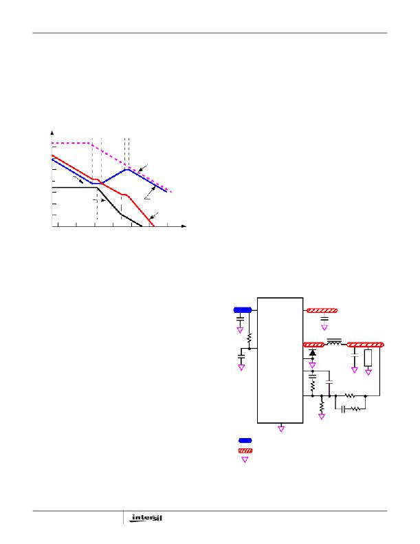
�FIGURE� 33.� ASYMPTOTIC� BODE� PLOT� OF� CONVERTER� GAIN�
�Layout� Considerations�
�Layout� is� very� important� in� high� frequency� switching�
�converter� design.� With� power� devices� switching� efficiently� at�
�500kHz,� the� resulting� current� transitions� from� one� device� to�
�another� cause� voltage� spikes� across� the� interconnecting�
�The� critical� small� signal� components� include� any� bypass�
�capacitors,� feedback� components,� and� compensation�
�components.� Place� the� PWM� converter� compensation�
�components� close� to� the� FB� and� COMP� pins.� The� feedback�
�resistors� should� be� located� as� close� as� possible� to� the� FB�
�pin� with� vias� tied� straight� to� the� ground� plane� as� required.�
�impedances� and� parasitic� circuit� elements.� These� voltage�
�spikes� can� degrade� efficiency,� radiate� noise� into� the� circuit,�
�and� lead� to� device� overvoltage� stress.� Careful� component�
�layout� and� printed� circuit� board� design� minimizes� these�
�5V�
�C� BP1�
�PVCC�
�ISL8501�
�VIN�
�V� IN�
�C� IN�
�voltage� spikes.�
�As� an� example,� consider� the� turn-off� transition� of� the� upper�
�MOSFET.� Prior� to� turn-off,� the� MOSFET� is� carrying� the� full�
�R� BP�
�C� BP2�
�VCC�
�PHASE�
�PGND�
�D�
�L�
�C� OUT1�
�V� OUT1�
�load� current.� During� turn-off,� current� stops� flowing� in� the�
�MOSFET� and� is� picked� up� by� the� Schottky� diode.� Any�
�parasitic� inductance� in� the� switched� current� path� generates� a�
�large� voltage� spike� during� the� switching� interval.� Careful�
�COMP�
�C� 2�
�R� 2�
�C� 1�
�R� 1�
�component� selection,� tight� layout� of� the� critical� components,�
�FB�
�and� short,� wide� traces� minimizes� the� magnitude� of� voltage�
�R� 4�
�C� 3�
�R� 3�
�spikes.�
�GND� PAD�
�There� are� two� sets� of� critical� components� in� the� ISL8501�
�switching� converter.� The� switching� components� are� the� most�
�critical� because� they� switch� large� amounts� of� energy,� and�
�therefore� tend� to� generate� large� amounts� of� noise.� Next� are�
�the� small� signal� components,� which� connect� to� sensitive�
�nodes� or� supply� critical� bypass� current� and� signal� coupling.�
�A� multi-layer� printed� circuit� board� is� recommended.� Figure� 34�
�shows� the� connections� of� the� critical� components� in� the�
�converter.� Note� that� capacitors� C� IN� and� C� OUT� could� each�
�18�
�KEY�
�ISLAND� ON� POWER� PLANE� LAYER�
�ISLAND� ON� CIRCUIT� AND/OR� POWER� PLANE� LAYER�
�VIA� CONNECTION� TO� GROUND� PLANE�
�FIGURE� 34.� PRINTED� CIRCUIT� BOARD� POWER� PLANES�
�AND� ISLANDS�
�FN6500.1�
�July� 12,� 2007�
�相关PDF资料 |
PDF描述 |
|---|---|
| ISL8510EVAL1Z | EVALUATION BOARD FOR ISL8510 |
| ISL89162FBEBZ | IC MOSFET DRIVER 2CH 6A 8SOIC |
| ISL89165FBECZ | MOSFET DRIVER 2CH 6A 8SOIC |
| ISL89168FBEAZ | IC MOSFET DRIVER 2CH 6A 8SOIC |
| ISL89367FRTAZ | IC MOSFET DRIVER 2CH 6A 16TDFN |
相关代理商/技术参数 |
参数描述 |
|---|---|
| ISL8501IRZ | 功能描述:电压模式 PWM 控制器 INTEGRTD FETUCK 4X 4 24LD W/ANNEAL RoHS:否 制造商:Texas Instruments 输出端数量:1 拓扑结构:Buck 输出电压:34 V 输出电流: 开关频率: 工作电源电压:4.5 V to 5.5 V 电源电流:600 uA 最大工作温度:+ 125 C 最小工作温度:- 40 C 封装 / 箱体:WSON-8 封装:Reel |
| ISL8501IRZ-T | 功能描述:电压模式 PWM 控制器 INTEGRTD FETUCK 4X 4 24LD W/ANNEAL RoHS:否 制造商:Texas Instruments 输出端数量:1 拓扑结构:Buck 输出电压:34 V 输出电流: 开关频率: 工作电源电压:4.5 V to 5.5 V 电源电流:600 uA 最大工作温度:+ 125 C 最小工作温度:- 40 C 封装 / 箱体:WSON-8 封装:Reel |
| ISL8502AEVAL1Z | 功能描述:EVAL BOARD FOR ISL8502 RoHS:是 类别:编程器,开发系统 >> 评估板 - DC/DC 与 AC/DC(离线)SMPS 系列:- 产品培训模块:Obsolescence Mitigation Program 标准包装:1 系列:True Shutdown™ 主要目的:DC/DC,步升 输出及类型:1,非隔离 功率 - 输出:- 输出电压:- 电流 - 输出:1A 输入电压:2.5 V ~ 5.5 V 稳压器拓扑结构:升压 频率 - 开关:3MHz 板类型:完全填充 已供物品:板 已用 IC / 零件:MAX8969 |
| ISL8502AIRZ | 功能描述:IC REG BUCK SYNC ADJ 2A 24QFN RoHS:是 类别:集成电路 (IC) >> PMIC - 稳压器 - DC DC 开关稳压器 系列:- 产品培训模块:Lead (SnPb) Finish for COTS Obsolescence Mitigation Program 标准包装:2,500 系列:- 类型:降压(降压) 输出类型:两者兼有 输出数:1 输出电压:5V,1 V ~ 10 V 输入电压:3.5 V ~ 28 V PWM 型:电流模式 频率 - 开关:220kHz ~ 1MHz 电流 - 输出:600mA 同步整流器:无 工作温度:-40°C ~ 125°C 安装类型:表面贴装 封装/外壳:16-SSOP(0.154",3.90mm 宽) 包装:带卷 (TR) 供应商设备封装:16-QSOP |
| ISL8502AIRZ-T | 功能描述:IC REG BUCK SYNC ADJ 2A 24QFN RoHS:是 类别:集成电路 (IC) >> PMIC - 稳压器 - DC DC 开关稳压器 系列:- 产品培训模块:Lead (SnPb) Finish for COTS Obsolescence Mitigation Program 标准包装:2,500 系列:- 类型:降压(降压) 输出类型:两者兼有 输出数:1 输出电压:5V,1 V ~ 10 V 输入电压:3.5 V ~ 28 V PWM 型:电流模式 频率 - 开关:220kHz ~ 1MHz 电流 - 输出:600mA 同步整流器:无 工作温度:-40°C ~ 125°C 安装类型:表面贴装 封装/外壳:16-SSOP(0.154",3.90mm 宽) 包装:带卷 (TR) 供应商设备封装:16-QSOP |
发布紧急采购,3分钟左右您将得到回复。