- 您现在的位置:买卖IC网 > PDF目录20546 > ISL89367FRTAZ-T (Intersil)IC MOSFET DRIVER 2CH 6A 16TDFN PDF资料下载
参数资料
| 型号: | ISL89367FRTAZ-T |
| 厂商: | Intersil |
| 文件页数: | 10/14页 |
| 文件大小: | 0K |
| 描述: | IC MOSFET DRIVER 2CH 6A 16TDFN |
| 标准包装: | 4,000 |
| 配置: | 低端 |
| 输入类型: | 与和反相 |
| 延迟时间: | 25ns |
| 配置数: | 2 |
| 输出数: | 2 |
| 电源电压: | 4.5 V ~ 16 V |
| 工作温度: | -40°C ~ 125°C |
| 安装类型: | 表面贴装 |
| 封装/外壳: | 16-WFDFN 裸露焊盘 |
| 供应商设备封装: | 16-TDFN |
| 包装: | 带卷 (TR) |
�� �
�
�ISL89367�
�t� delay� =� R� b� � C�
�Functional� Description�
�Overview�
�Note:� In� the� following� discussion,� when� a� lower� case� “n”� or� “x”� is�
�used� in� a� pin� name,� the� “n”� can� be� replaced� by� “1”� or� “2”� and� “x”�
�can� be� replaced� by� “A”� or� “B”.�
�The� ISL89367� drivers� are� designed� specifically� for� Synchronous�
�Rectifier� (SR)� applications� but� can� also� be� used� for� any� MOSFET�
�driver� application� especially� when� a� precision� propagation� time�
�delay� is� required� for� the� output� rising� for� falling� edge� (or� both).�
�The� fast� rising� (or� falling)� output� drive� current� of� the� ISL89367�
�minimizes� the� turn-on� (or� off)� delay� due� to� the� input� capacitance�
�of� the� driven� FET.� The� switching� transition� period� at� the� Miller�
�plateau� is� also� minimized� by� the� high� amplitude� drive� currents.�
�(See� the� specified� Miller� plateau� currents� in� the� AC� Electrical�
�Specifications� on� page� 6).�
�The� start-up� sequence� for� is� designed� to� prevent� unexpected�
�glitches� when� V� DD� is� being� turned� on� or� turned� off.� When�
�V� DD� <� ~1V,� an� internal� 10k� ?� resistor� connected� between� the�
�output� and� ground,� help� to� keep� the� gate� voltage� close� to� ground.�
�When� ~1V� <� V� DD� <� UV,� both� outputs� are� driven� low� while� ignoring�
�the� logic� inputs.� This� low� state� has� the� same� current� sinking�
�capacity� as� during� normal� operation.� This� insures� that� the� driven�
�FETs� are� held� off� even� if� there� is� a� switching� voltage� on� the� drains�
�that� can� inject� charge� into� the� gates� via� the� Miller� capacitance.�
�When� V� DD� >� UVLO,� and� after� a� 400μs� delay,� the� outputs� now�
�respond� to� the� logic� inputs.� See� Figure� 9� for� complete� details.�
�For� the� negative� transition� of� V� DD� through� the� UV� lockout� voltage,�
�the� outputs� are� active� low� when� V� DD� <� ~3.2V� DC� regardless� of� the�
�input� logic� states.�
�Input� Logic� Voltage� Levels�
�The� input� logic� (INnx)� has� thresholds� of� 37%� (falling� input)� and�
�linearly� between� ~40ns� and� ~265ns� for� values� from� 2k� ?� to�
�20k� ?� .� If� no� time� delay� is� required,� short� RDELx� and� FDELx� to� VSS.�
�Programmed� delays� for� resistor� values� <2k� are� not� specified� or�
�recommended.� Resistor� values� >20k� are� also� not� recommended.�
�Delays� Greater� than� 270ns�
�For� application� requiring� delay� durations� longer� than� 270ns,� the�
�ISL89367� also� offers� a� solution.� The� input� logic� pins� have�
�precision� thresholds� which� are� designed� for� precision� time� delays�
�of� either� the� rising� of� falling� edge� of� OUTx� by� using� the� time�
�constant� of� a� resistor� and� capacitor.� The� logic� inputs� pins� of� the�
�driver,� INnx,� are� connected� to� the� positive� inputs� of� the� input�
�comparators.� The� positive� and� negative� transition� threshold�
�voltages� are� established� on� the� negative� inputs� of� these�
�comparator� by� a� resistor� divider� that� is� biased� by� V� REF+� and�
�V� REF-� .� If� V� REF+� is� connected� to� the� bias� voltage� of� the� input� logic�
�and� if� V� REF-� is� connected� to� the� ground� of� the� input� logic,� then�
�the� threshold� transitions� are� proportional� to� the� bias� voltage� of�
�the� input� logic.� Consequently,� the� time� delays� are� independent� of�
�the� accuracy� of� the� input� logic� bias� voltage.�
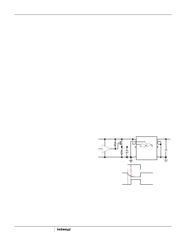
�Figure� 17� illustrates� a� circuit� that� is� used� to� delay� the� rising� edge�
�of� OUTA� relative� to� the� rising� edge� of� the� signal� source.� The� value�
�of� C� should� also� be� substantially� larger� than� the� input�
�capacitance� of� the� input� pin� of� the� ISL89367,� the� parasitic�
�capacitance� associated� with� the� traces,� and� the� output�
�capacitance,� C� DS� of� the� signal� FET� Q1.�
�If� the� signal� source� is� TTL� or� open� drain,� R� a� is� required� but� not� for�
�CMOS.�
�The� calculation� of� the� rising� delay� is� simply� shown� by� Equation� 1:�
�(EQ.� 1)�
�This� is� a� consequence� of� the� 37%/63%� thresholds.�
�FDELA�
�63%� (rising� input).� The� maximum� V� REF+� relative� to� V� REF-� is�
�10V� DC� .� For� typical� 5V� logic� applications� V� REF+� =� 5V,� V� REF-� =� 0V.�
�In� a� similar� manner,� applications� with� 3.3V� logic� V� REF+� =� 3.3V�
�and� V� REF-� =� 0V.� Note� that� the� INVx� inputs� have� TTL� compatible�
�thresholds,� are� V� DD� tolerant,� and� do� not� have� precision�
�thresholds.�
�R� a�
�SIGNAL�
�SOURCE�
�Q1�
�R� b�
�C�
�VREF+� VDD�
�INVA�
�IN1A� RDELA�
�IN2A� OUTA�
�ISL89367�
�only� section� A� is� shown�
�VREF-� VSS�
�Programmable� Delays�
�The� propagation� time� delays� are� programmed� by� resistors�
�connected� between� RDELx� or� FDELx� and� VSS.� A� resistor�
�connected� to� RDELx� delays� the� rising� edge� of� OUTx.� Likewise,� a�
�resistor� connected� to� FDELx� delays� the� falling� edge� of� OUTx.� The�
�resistors� should� be� connected� as� close� as� possible� to� the� pins� to�
�prevent� noise� coupling� into� these� connections.� In� extremely� noisy�
�applications,� it� may� be� necessary� to� bypass� the� resistors� with� a�
�0.01μF� or� smaller� decoupling� capacitor.� The� time� delay� varies�
�10�
�SIGNAL�
�SOURCE�
�IN2A�
�OUTA�
�FIGURE� 17.� RISING� OUTA� TIME� DELAY�
�FN7727.1�
�October� 8,� 2012�
�相关PDF资料 |
PDF描述 |
|---|---|
| 396-056-522-204 | CARD EDGE 56POS DL .125X.250 BLK |
| T95V475M016HSAL | CAP TANT 4.7UF 16V 20% 1410 |
| SBG3040CT-T-F | DIODE SCHOTTKY 30A 40V D2PAK |
| RKZ-1205S/H | CONV DC/DC 2W 12VIN 05VOUT |
| ISL6614IRZR5238 | IC DRVR DUAL SYNC BUCK 16-QFN |
相关代理商/技术参数 |
参数描述 |
|---|---|
| ISL89400ABZ | 功能描述:IC DRVR H-BRDG 100V 1.25A 8SOIC RoHS:是 类别:集成电路 (IC) >> PMIC - MOSFET,电桥驱动器 - 外部开关 系列:- 标准包装:6,000 系列:* |
| ISL89400ABZ-T | 功能描述:IC DRVR H-BRDG 100V 1.25A 8SOIC RoHS:是 类别:集成电路 (IC) >> PMIC - MOSFET,电桥驱动器 - 外部开关 系列:- 标准包装:6,000 系列:* |
| ISL89400ABZ-TK | 功能描述:IC DRVR H-BRDG 100V 1.25A 8SOIC RoHS:是 类别:集成电路 (IC) >> PMIC - MOSFET,电桥驱动器 - 外部开关 系列:- 标准包装:6,000 系列:* |
| ISL89400AR3Z | 功能描述:IC MOSFET DRVR 100V 1.25A 9-DFN RoHS:是 类别:集成电路 (IC) >> PMIC - MOSFET,电桥驱动器 - 外部开关 系列:- 标准包装:6,000 系列:* |
| ISL89400AR3Z-T | 功能描述:IC MOSFET DRVR 100V 1.25A 9-DFN RoHS:是 类别:集成电路 (IC) >> PMIC - MOSFET,电桥驱动器 - 外部开关 系列:- 标准包装:6,000 系列:* |
发布紧急采购,3分钟左右您将得到回复。