- 您现在的位置:买卖IC网 > PDF目录20546 > ISL89367FRTAZ-T (Intersil)IC MOSFET DRIVER 2CH 6A 16TDFN PDF资料下载
参数资料
| 型号: | ISL89367FRTAZ-T |
| 厂商: | Intersil |
| 文件页数: | 11/14页 |
| 文件大小: | 0K |
| 描述: | IC MOSFET DRIVER 2CH 6A 16TDFN |
| 标准包装: | 4,000 |
| 配置: | 低端 |
| 输入类型: | 与和反相 |
| 延迟时间: | 25ns |
| 配置数: | 2 |
| 输出数: | 2 |
| 电源电压: | 4.5 V ~ 16 V |
| 工作温度: | -40°C ~ 125°C |
| 安装类型: | 表面贴装 |
| 封装/外壳: | 16-WFDFN 裸露焊盘 |
| 供应商设备封装: | 16-TDFN |
| 包装: | 带卷 (TR) |
�� �
�
�ISL89367�
�R� a�
�R� b�
�VREF+�
�INVA�
�IN1A�
�VDD�
�FDELA�
�RDELA�
�12�
�10�
�I� D� = 12A�
�V� DS� = 0V�
�IN2A�
�OUTA�
�SIGNAL�
�SOURCE�
�Q1�
�C�
�ISL89367�
�only� section� A� is� shown�
�VREF-� VSS�
�8�
�6�
�V� DS� = 64V�
�V� DS� = 40V�
�4�
�SIGNAL�
�SOURCE�
�2�
�IN2A�
�0�
�0�
�2�
�4� 6� 8� 10� 12� 14� 16� 18� 20� 22� 24�
�QG,� TOTAL� GATE� CHARGE� (nC)�
�OUTA�
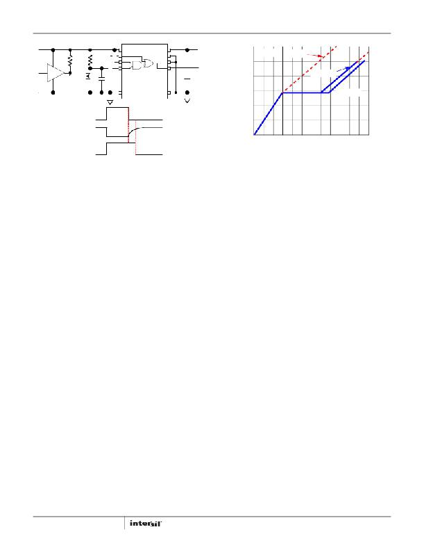
�FIGURE� 18.� FALLING� OUTA� TIME� DELAY�
�Figure� 18� is� used� to� delay� the� falling� edge� of� OUTx.� In� this� case�
�the� rising� time� constant� is� R� b� x� C.�
�Logic� States�
�The� combinational� control� logic� of� the� ISL89367� is� very� flexible.�
�The� state� of� OUTx� is� the� ANDed� logic� of� both� inputs,� IN1x� and�
�IN2x.� The� INVx� input� to� the� exclusive-OR� gate� is� used� to� invert� the�
�logic� state� of� OUTx.� Frequently,� for� SR� applications,� it� is� desirable�
�to� have� a� logic� control� that� can� force� OUTA� =� 0� for� the� purpose� of�
�diode� emulation.� This� “enable”� control� input� can� be� either� of� the�
�IN1x� or� IN2x� inputs� of� one� channel.� In� Figure� 1� on� page� 1,� IN1A� is�
�used� as� the� enabled� input� for� channel� A.� When� this� input� is� tied�
�to� V� REF+� ,� OUTA� follows� the� state� of� IN2x.� If� INA1� is� connected� to�
�V� REF-� ,� with� INVA� =� 0,� OUTA� remains� low� no� matter� what� state�
�IN2A� is� in.�
�FIGURE� 19.� CHARGE� OF� A� TYPICAL� MOSFET�
�Figure� 19� illustrates� how� the� gate� charge� varies� with� gate�
�voltage,� V� GS� ,� and� the� V� DS� of� the� driven� MOSFET.� Because� an� SR�
�is� switched� on� and� off� when� V� DS� =� 0� and� if� we� use� V� GS� =� 12V,�
�from� the� graph,� Q� G� =� 13.5nC.� In� this� example� the� dissipation� of�
�the� driver� with� frequency� =� 1MHz� is� shown� by� Equation� 2:�
�P� gate� =� 2� � Qg� � freq� � V� GS� (EQ.� 2)�
�=� 2� � 17nC� � 1MHz� � 12�
�=� 0.408W�
�Notice� that� the� dissipation� of� the� driver� is� not� a� function� of� the�
�peak� drive� rating� of� the� driver.� Also� if� an� external� gate� resistor� is�
�used� to� limit� the� peak� current� output,� the� dissipation� is�
�proportionally� shared� between� the� value� of� the� gate� resistor� and�
�the� r� DS(ON)� of� the� ISL89367� output.�
�Another� parameter� that� must� be� considered� is� the� dissipation�
�resulting� from� the� bias� current� at� the� frequency� of� operation.� For�
�the� ISL89367� the� bias� current� @� V� DD� =� 12V� and� 1MHz� is� 24mA.�
�Paralleling� Outputs� to� Double� the� Peak� Drive�
�Currents�
�The� typical� propagation� matching� of� the� ISL89367� is� less� than�
�1ns.� Note� that� the� propagation� matching� is� only� valid� when�
�FDELA� =� RDELA� =� 0k� ?� and� FDELB� =� RDELB� =� 0k� ?� .� The� matching�
�is� so� precise� that� carefully� matched� and� calibrated� scopes�
�probes� and� scope� channels� must� be� used� to� make� this�
�measurement.� Because� of� this� excellent� performance,� these�
�driver� outputs� can� be� safely� paralleled� to� double� the� current� drive�
�capacity.� It� is� important� that� the� INA� and� INB� inputs� be�
�P� bias� =� V� DS� � I� bias� =� 12V� � 24mA� =� 0.288W�
�P� total� =� P� gate� +� P� bias� +� 0.408W� +� 0.288W� =� 0.696W�
�The� Thermal� impedances� of� the� ISL89367� are:�
�θ� JC� =� 3°C/W�
�θ� JA� =� 36°C/W�
�The� temperature� rise� is:�
�T� riseJC� =� θ� JC� ×� P� total� =� 2.09� Δ� C�
�(EQ.� 3)�
�(EQ.� 4)�
�(EQ.� 5)�
�connected� together� on� the� PCB� with� the� shortest� possible� trace.�
�This� is� also� required� of� OUTA� and� OUTB.�
�T� riseJC� is� the� temperature� rise� referenced� to� the� temperature� of�
�the� PCB� ground� plane� under� the� part.�
�Power� Dissipation� and� Die� Temp�
�T� riseJA� =� θ� JA� ×� P� total� =� 25� Δ� C�
�(EQ.� 6)�
�The� following� is� an� example� of� how� to� calculate� the� power�
�dissipated� by� the� ISL89367� driver.� These� calculations� are�
�intended� to� give� an� approximate� temperature� rise� of� the� die�
�junction.� Because� operating� conditions� such� as� air� flow� can�
�influence� the� actual� temperatures,� it� is� absolutely� necessary� to�
�confirm� the� operating� temperatures� in� a� specific� application� by�
�measuring� the� ISL89367� temperatures� with� an� infra-red�
�temperature� sensor� or� camera.� Using� a� thermal� couple� to�
�measure� the� temperature� of� small� devices� is� not� recommended�
�because� the� thermal� couple� wire� will� act� as� a� heat� sink� reducing�
�the� temperature� of� the� measured� device� to� values� less� than� what�
�will� actually� occur.� See� Tech� Brief� TB379� for� more� information.�
�11�
�In� this� example� the� temperature� rise� is� relatively� small� for� θ� JC�
�and� θ� JA� .� Obviously� the� ISL89367� could� drive� significantly� larger�
�FETs� than� what� is� used� in� this� example.�
�Output� Current� Rating�
�While� the� ISL89367� has� a� very� high� peak� output� current� rating� of�
�6A� sourcing� and� sinking,� there� are� limitations� to� the� average�
�output� current.� With� the� high� peak� output� current� of� the�
�ISL89367,� it� is� tempting� to� use� the� driver� as� a� general� purpose�
�switch� to� drive� loads� that� are� not� capacitive� as� are� the� gates� of�
�MOSFETs.� It� is� important� to� note� that� the� maximum� average�
�output� current� rating� of� the� ISL89367� of� 150mA� must� not� be�
�FN7727.1�
�October� 8,� 2012�
�相关PDF资料 |
PDF描述 |
|---|---|
| 396-056-522-204 | CARD EDGE 56POS DL .125X.250 BLK |
| T95V475M016HSAL | CAP TANT 4.7UF 16V 20% 1410 |
| SBG3040CT-T-F | DIODE SCHOTTKY 30A 40V D2PAK |
| RKZ-1205S/H | CONV DC/DC 2W 12VIN 05VOUT |
| ISL6614IRZR5238 | IC DRVR DUAL SYNC BUCK 16-QFN |
相关代理商/技术参数 |
参数描述 |
|---|---|
| ISL89400ABZ | 功能描述:IC DRVR H-BRDG 100V 1.25A 8SOIC RoHS:是 类别:集成电路 (IC) >> PMIC - MOSFET,电桥驱动器 - 外部开关 系列:- 标准包装:6,000 系列:* |
| ISL89400ABZ-T | 功能描述:IC DRVR H-BRDG 100V 1.25A 8SOIC RoHS:是 类别:集成电路 (IC) >> PMIC - MOSFET,电桥驱动器 - 外部开关 系列:- 标准包装:6,000 系列:* |
| ISL89400ABZ-TK | 功能描述:IC DRVR H-BRDG 100V 1.25A 8SOIC RoHS:是 类别:集成电路 (IC) >> PMIC - MOSFET,电桥驱动器 - 外部开关 系列:- 标准包装:6,000 系列:* |
| ISL89400AR3Z | 功能描述:IC MOSFET DRVR 100V 1.25A 9-DFN RoHS:是 类别:集成电路 (IC) >> PMIC - MOSFET,电桥驱动器 - 外部开关 系列:- 标准包装:6,000 系列:* |
| ISL89400AR3Z-T | 功能描述:IC MOSFET DRVR 100V 1.25A 9-DFN RoHS:是 类别:集成电路 (IC) >> PMIC - MOSFET,电桥驱动器 - 外部开关 系列:- 标准包装:6,000 系列:* |
发布紧急采购,3分钟左右您将得到回复。