- 您现在的位置:买卖IC网 > PDF目录20546 > ISL89367FRTAZ-T (Intersil)IC MOSFET DRIVER 2CH 6A 16TDFN PDF资料下载
参数资料
| 型号: | ISL89367FRTAZ-T |
| 厂商: | Intersil |
| 文件页数: | 12/14页 |
| 文件大小: | 0K |
| 描述: | IC MOSFET DRIVER 2CH 6A 16TDFN |
| 标准包装: | 4,000 |
| 配置: | 低端 |
| 输入类型: | 与和反相 |
| 延迟时间: | 25ns |
| 配置数: | 2 |
| 输出数: | 2 |
| 电源电压: | 4.5 V ~ 16 V |
| 工作温度: | -40°C ~ 125°C |
| 安装类型: | 表面贴装 |
| 封装/外壳: | 16-WFDFN 裸露焊盘 |
| 供应商设备封装: | 16-TDFN |
| 包装: | 带卷 (TR) |
�� �
�
�ISL89367�
�Q� g� =� 150mA� ?� 1MHz� =� 150nC�
�P� gate� =� 2� � 150nC� � 1MHz� � 12V� =� 3.6W�
�overlooked.� While� this� value� seems� low,� it� is� more� than� adequate�
�to� drive� very� high� gate� charge� values� at� high� frequencies.�
�The� average� output� current� (sinking� or� sourcing)� into� a� capacitive�
�load� is:�
�I� avg� =� Qg� x� freq�
�or� Qg� =� I� avg� /freq�
�for� a� frequency� of� 1MHz� and� for� the� maximum� average� current� of�
�150mA:�
�(EQ.� 7)�
�This� charge� is� approximately� 10x� the� value� of� the� gate� charge� as�
�in� the� example� of� Figure� 2� on� page� 1.� Obviously,� with� lower�
�frequencies,� this� margin� is� even� greater.� It� is� likely� that� the�
�greater� limitation� of� driving� a� large� capacitive� load� could� be� the�
�power� dissipation.� If� the� driver� dissipation� is� recalculated� with� a�
�value� of� 150nC,� then:�
�(EQ.� 8)�
�?� It� may� be� necessary� to� add� resistance� to� dampen� resonating�
�parasitic� circuits� especially� on� OUTA� and� OUTB.� If� an� external�
�gate� resistor� is� unacceptable,� then� the� layout� must� be�
�improved� to� minimize� lead� inductance.�
�?� Keep� high� dv/dt� nodes� away� from� low� level� circuits.� Guard�
�banding� can� be� used� to� shunt� away� dv/dt� injected� currents�
�from� sensitive� circuits.� This� is� especially� true� for� control� circuits�
�that� source� the� input� signals� to� the� ISL89367.�
�?� Avoid� having� a� signal� ground� plane� under� a� high� amplitude�
�dv/dt� circuit.� This� will� inject� di/dt� currents� into� the� signal�
�ground� paths.�
�?� Do� power� dissipation� and� voltage� drop� calculations� of� the�
�power� traces.� Many� PCB/CAD� programs� have� built� in� tools� for�
�calculation� of� trace� resistance.�
�?� Large� power� components� (Power� FETs,� Electrolytic� caps,� power�
�resistors,� etc.)� will� have� internal� parasitic� inductance� which�
�cannot� be� eliminated.�
�This� must� be� accounted� for� in� the� PCB� layout� and� circuit�
�T� riseJA� =� 33� ×� 3.6W� =� 119� Δ� C�
�(EQ.� 9)�
�design.�
�?� If� you� simulate� your� circuits,� consider� including� parasitic�
�PCB� Layout� Guidelines�
�The� AC� performance� of� the� ISL89367� depends� significantly� on�
�the� design� of� the� PC� board.� The� following� layout� design�
�guidelines� are� recommended� to� achieve� optimum� performance:�
�?� Place� the� driver� as� close� as� possible� to� the� driven� power� FET.�
�?� Understand� where� the� switching� power� currents� flow.� The� high�
�amplitude� di/dt� currents� of� the� driven� power� FET� will� induce�
�significant� voltage� transients� on� the� associated� traces.�
�?� Keep� power� loops� as� short� as� possible� by� paralleling� the�
�source� and� return� traces.�
�?� Use� planes� where� practical;� they� are� usually� more� effective�
�than� parallel� traces.�
�components� especially� parasitic� inductance.�
�EPAD� Heatsinking�
�Considerations�
�The� thermal� pad� is� electrically� connected� to� the� GND� supply�
�through� the� IC� substrate.� The� EPAD� of� the� ISL89367� has� two�
�main� functions:� to� provide� a� quiet� GND� for� the� input� threshold�
�comparators� and� to� provide� heat� sinking� for� the� IC.� The� EPAD�
�must� be� connected� to� a� ground� plane� and� no� switching� currents�
�from� the� driven� FET� should� pass� through� the� ground� plane� under�
�the� IC.�
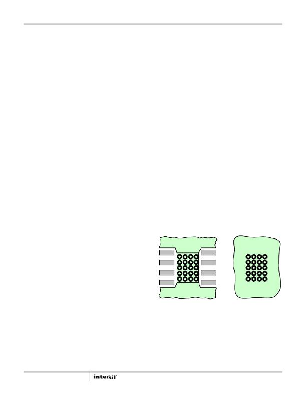
�Figure� 20� is� a� PCB� layout� example� of� how� to� use� vias� to� remove�
�heat� from� the� IC� through� the� EPAD.�
�?� Avoid� paralleling� high� amplitude� di/dt� traces� with� low� level�
�signal� lines.� High� di/dt� will� induce� currents� and� consequently,�
�noise� voltages� in� the� low� level� signal� lines.�
�?� When� practical,� minimize� impedances� in� low� level� signal�
�circuits.� The� noise,� magnetically� induced� on� a� 10k� resistor,� is�
�10x� larger� than� the� noise� on� a� 1k� resistor.�
�?� Be� aware� of� magnetic� fields� emanating� from� transformers� and�
�inductors.� Gaps� in� these� structures� are� especially� bad� for�
�emitting� flux.�
�?� If� you� must� have� traces� close� to� magnetic� devices,� align� the�
�EPAD� GND�
�PLANE�
�COMPONENT�
�LAYER�
�EPAD� GND�
�PLANE�
�BOTTOM�
�LAYER�
�traces� so� that� they� are� parallel� to� the� flux� lines� to� minimize�
�coupling.�
�?� The� use� of� low� inductance� components� such� as� chip� resistors�
�and� chip� capacitors� is� highly� recommended.�
�?� Use� decoupling� capacitors� to� reduce� the� influence� of� parasitic�
�inductance� in� the� VDD� and� GND� leads.� To� be� effective,� these�
�caps� must� also� have� the� shortest� possible� conduction� paths.� If�
�vias� are� used,� connect� several� paralleled� vias� to� reduce� the�
�inductance� of� the� vias.�
�12�
�FIGURE� 20.� TYPICAL� PCB� PATTERN� FOR� THERMAL� VIAS�
�For� maximum� heatsinking,� it� is� recommended� that� a� ground�
�plane,� connected� to� the� EPAD,� be� added� to� both� sides� of� the� PCB.�
�A� via� array,� within� the� area� of� the� EPAD,� will� conduct� heat� from�
�the� EPAD� to� the� GND� plane� on� the� bottom� layer.� The� number� of�
�vias� and� the� size� of� the� GND� planes� required� for� adequate�
�heatsinking� is� determined� by� the� power� dissipated� by� the�
�ISL89367,� the� air� flow� and� the� maximum� temperature� of� the� air�
�around� the� IC.�
�FN7727.1�
�October� 8,� 2012�
�相关PDF资料 |
PDF描述 |
|---|---|
| 396-056-522-204 | CARD EDGE 56POS DL .125X.250 BLK |
| T95V475M016HSAL | CAP TANT 4.7UF 16V 20% 1410 |
| SBG3040CT-T-F | DIODE SCHOTTKY 30A 40V D2PAK |
| RKZ-1205S/H | CONV DC/DC 2W 12VIN 05VOUT |
| ISL6614IRZR5238 | IC DRVR DUAL SYNC BUCK 16-QFN |
相关代理商/技术参数 |
参数描述 |
|---|---|
| ISL89400ABZ | 功能描述:IC DRVR H-BRDG 100V 1.25A 8SOIC RoHS:是 类别:集成电路 (IC) >> PMIC - MOSFET,电桥驱动器 - 外部开关 系列:- 标准包装:6,000 系列:* |
| ISL89400ABZ-T | 功能描述:IC DRVR H-BRDG 100V 1.25A 8SOIC RoHS:是 类别:集成电路 (IC) >> PMIC - MOSFET,电桥驱动器 - 外部开关 系列:- 标准包装:6,000 系列:* |
| ISL89400ABZ-TK | 功能描述:IC DRVR H-BRDG 100V 1.25A 8SOIC RoHS:是 类别:集成电路 (IC) >> PMIC - MOSFET,电桥驱动器 - 外部开关 系列:- 标准包装:6,000 系列:* |
| ISL89400AR3Z | 功能描述:IC MOSFET DRVR 100V 1.25A 9-DFN RoHS:是 类别:集成电路 (IC) >> PMIC - MOSFET,电桥驱动器 - 外部开关 系列:- 标准包装:6,000 系列:* |
| ISL89400AR3Z-T | 功能描述:IC MOSFET DRVR 100V 1.25A 9-DFN RoHS:是 类别:集成电路 (IC) >> PMIC - MOSFET,电桥驱动器 - 外部开关 系列:- 标准包装:6,000 系列:* |
发布紧急采购,3分钟左右您将得到回复。