- 您现在的位置:买卖IC网 > PDF目录9096 > ISPPAC-CLK5312S-01T48I (Lattice Semiconductor Corporation)IC BUFFER FANOUT ISP UNIV 48TQFP PDF资料下载
参数资料
| 型号: | ISPPAC-CLK5312S-01T48I |
| 厂商: | Lattice Semiconductor Corporation |
| 文件页数: | 15/56页 |
| 文件大小: | 0K |
| 描述: | IC BUFFER FANOUT ISP UNIV 48TQFP |
| 标准包装: | 250 |
| 系列: | ispClock™ |
| 类型: | 时钟发生器,扇出配送,零延迟缓冲器 |
| PLL: | 带旁路 |
| 输入: | HSTL,LVCMOS,LVDS,LVPECL,LVTTL,SSTL |
| 输出: | eHSTL,HSTL,LVCMOS,LVTTL,SSTL |
| 电路数: | 1 |
| 比率 - 输入:输出: | 2:12 |
| 差分 - 输入:输出: | 是/无 |
| 频率 - 最大: | 267MHz |
| 除法器/乘法器: | 是/无 |
| 电源电压: | 3 V ~ 3.6 V |
| 工作温度: | -40°C ~ 85°C |
| 安装类型: | 表面贴装 |
| 封装/外壳: | 48-LQFP |
| 供应商设备封装: | 48-TQFP(7x7) |
| 包装: | 托盘 |
第1页第2页第3页第4页第5页第6页第7页第8页第9页第10页第11页第12页第13页第14页当前第15页第16页第17页第18页第19页第20页第21页第22页第23页第24页第25页第26页第27页第28页第29页第30页第31页第32页第33页第34页第35页第36页第37页第38页第39页第40页第41页第42页第43页第44页第45页第46页第47页第48页第49页第50页第51页第52页第53页第54页第55页第56页
Lattice Semiconductor
ispClock5300S Family Data Sheet
22
LVTTL (3.3V), LVCMOS (1.8V, 2.5V, 3.3V)
The receiver should be set to LVCMOS or LVTTL mode, and the input signal can be connected to either the REFA
or REFB pins. CMOS transmission lines are generally source terminated, so all termination resistors should be set
to the OPEN state. Figure 15 shows the proper conguration. Please note that because switching thresholds are
different for LVCMOS running at 1.8V, there is a separate conguration setting for this particular standard. Unused
reference inputs and VTT pins should be grounded.
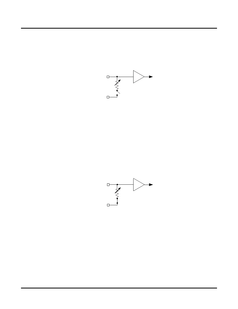
Figure 15. LVCMOS/LVTTL Input Receiver Conguration
HSTL, eHSTL, SSTL2, SSTL3
The receiver should be set to HSTL/SSTL mode, and the input signal can be connected to the REFA or REFB ter-
minal of the input pair and the associated VTT_REFA or VTT_REFB terminal should be tied to a VTT termination
supply. The terminating resistor should be set to 50Ω and the engaging switch should be closed. Figure 16 shows
an appropriate conguration. Refer to the “Recommended Operating Conditions - Supported Logic Standards”
table in this data sheet for suitable values of VREF and VTT.
One important point to note is that the termination supplies must have low impedance and be able to both source
and sink current without experiencing uctuations. These requirements generally preclude the use of a resistive
divider network, which has an impedance comparable to the resistors used, or of commodity-type linear voltage
regulators, which can only source current. The best way to develop the necessary termination voltages is with a
regulator specically designed for this purpose. Because SSTL and HSTL logic is commonly used for high-perfor-
mance memory busses, a suitable termination voltage supply is often already available in the system.
Figure 16. SSTL2, SSTL3, eHSTL, HSTL Receiver Conguration
Differential LVPECL/LVDS
The receiver should be set to LVDS or LVPECL mode as required and both termination resistors should be
engaged and set to 50Ω. The VTT_REFA and VTT_REFB pins, however, should be connected. This creates a oat-
ing 100Ω differential termination resistance across the input terminals. The LVDS termination conguration is
shown in Figure 17.
Note: the REFSEL pin should be grounded when the input receiver is congured as differential.
Single-ended
Receiver
Open
GND
RT
VTT_REFA /
VTT_REFB
REFA_REFP /
REFB_REFN
Single-ended
Receiver
Closed
50
VTT_REFA /
VTT_REFB
REFA_REFP /
REFB_REFN
相关PDF资料 |
PDF描述 |
|---|---|
| ISPPAC-CLK5312S-01TN48I | IC CLOCK PROGRAM BUFFER 48TQFP |
| VI-27Z-MX-F2 | CONVERTER MOD DC/DC 2V 30W |
| X9317TM8I-2.7T2 | IC XDCP 100TAP 100K 3WIRE 8-MSOP |
| X9314WST1 | IC XDCP SGL 32-TAP 10K 8-SOIC |
| ISPPAC-CLK5316S-01T64C | IC BUFFER FANOUT ISP UNIV 64TQFP |
相关代理商/技术参数 |
参数描述 |
|---|---|
| ISPPACCLK5312S-01T48I | 制造商:LATTICE 制造商全称:Lattice Semiconductor 功能描述:In-System Programmable, Zero-Delay, Universal Fan-Out Buffer, Single-Ended |
| ISPPACCLK5312S-01T64C | 制造商:LATTICE 制造商全称:Lattice Semiconductor 功能描述:In-System Programmable, Zero-Delay, Universal Fan-Out Buffer, Single-Ended |
| ISPPACCLK5312S-01T64I | 制造商:LATTICE 制造商全称:Lattice Semiconductor 功能描述:In-System Programmable, Zero-Delay, Universal Fan-Out Buffer, Single-Ended |
| ispPAC-CLK5312S-01TN48C | 功能描述:时钟驱动器及分配 ISP 0 Delay Unv Fan- Out Buf-Sngl End RoHS:否 制造商:Micrel 乘法/除法因子:1:4 输出类型:Differential 最大输出频率:4.2 GHz 电源电压-最大: 电源电压-最小:5 V 最大工作温度:+ 85 C 封装 / 箱体:SOIC-8 封装:Reel |
| ISPPACCLK5312S-01TN48C | 制造商:LATTICE 制造商全称:Lattice Semiconductor 功能描述:In-System Programmable, Zero-Delay, Universal Fan-Out Buffer, Single-Ended |
发布紧急采购,3分钟左右您将得到回复。