- 您现在的位置:买卖IC网 > PDF目录9096 > ISPPAC-CLK5312S-01T48I (Lattice Semiconductor Corporation)IC BUFFER FANOUT ISP UNIV 48TQFP PDF资料下载
参数资料
| 型号: | ISPPAC-CLK5312S-01T48I |
| 厂商: | Lattice Semiconductor Corporation |
| 文件页数: | 17/56页 |
| 文件大小: | 0K |
| 描述: | IC BUFFER FANOUT ISP UNIV 48TQFP |
| 标准包装: | 250 |
| 系列: | ispClock™ |
| 类型: | 时钟发生器,扇出配送,零延迟缓冲器 |
| PLL: | 带旁路 |
| 输入: | HSTL,LVCMOS,LVDS,LVPECL,LVTTL,SSTL |
| 输出: | eHSTL,HSTL,LVCMOS,LVTTL,SSTL |
| 电路数: | 1 |
| 比率 - 输入:输出: | 2:12 |
| 差分 - 输入:输出: | 是/无 |
| 频率 - 最大: | 267MHz |
| 除法器/乘法器: | 是/无 |
| 电源电压: | 3 V ~ 3.6 V |
| 工作温度: | -40°C ~ 85°C |
| 安装类型: | 表面贴装 |
| 封装/外壳: | 48-LQFP |
| 供应商设备封装: | 48-TQFP(7x7) |
| 包装: | 托盘 |
第1页第2页第3页第4页第5页第6页第7页第8页第9页第10页第11页第12页第13页第14页第15页第16页当前第17页第18页第19页第20页第21页第22页第23页第24页第25页第26页第27页第28页第29页第30页第31页第32页第33页第34页第35页第36页第37页第38页第39页第40页第41页第42页第43页第44页第45页第46页第47页第48页第49页第50页第51页第52页第53页第54页第55页第56页
Lattice Semiconductor
ispClock5300S Family Data Sheet
24
actual impedance required will be a function of the driver used to generate the signal and the transmission medium
used (PCB traces, connectors and cabling). The ispClock5300S’s ability to adjust input impedance over a range of
40Ω to 70Ω allows the user to adapt his circuit to non-ideal behaviors from the rest of the system without having to
swap out components.
Output Drivers
The ispClock5300S provides multiple banks, with each bank supporting two high-speed clock outputs which are
congurable and internally terminated. There are ten banks in the ispClock5320S, eight banks in the
ispClock5316S, six banks in the ispClock5312S, four banks in the ispClock5308S and two banks in the
ispClock5304S. Programmable internal source-series termination allows the ispClock5300S to be matched to
transmission lines with impedances ranging from 40 to 70Ω. The outputs may be independently enabled or dis-
abled, either from E
2CMOS conguration or by external control lines. Additionally, each can be independently pro-
grammed to provide a xed amount of signal delay or skew, allowing the user to compensate for the effects of
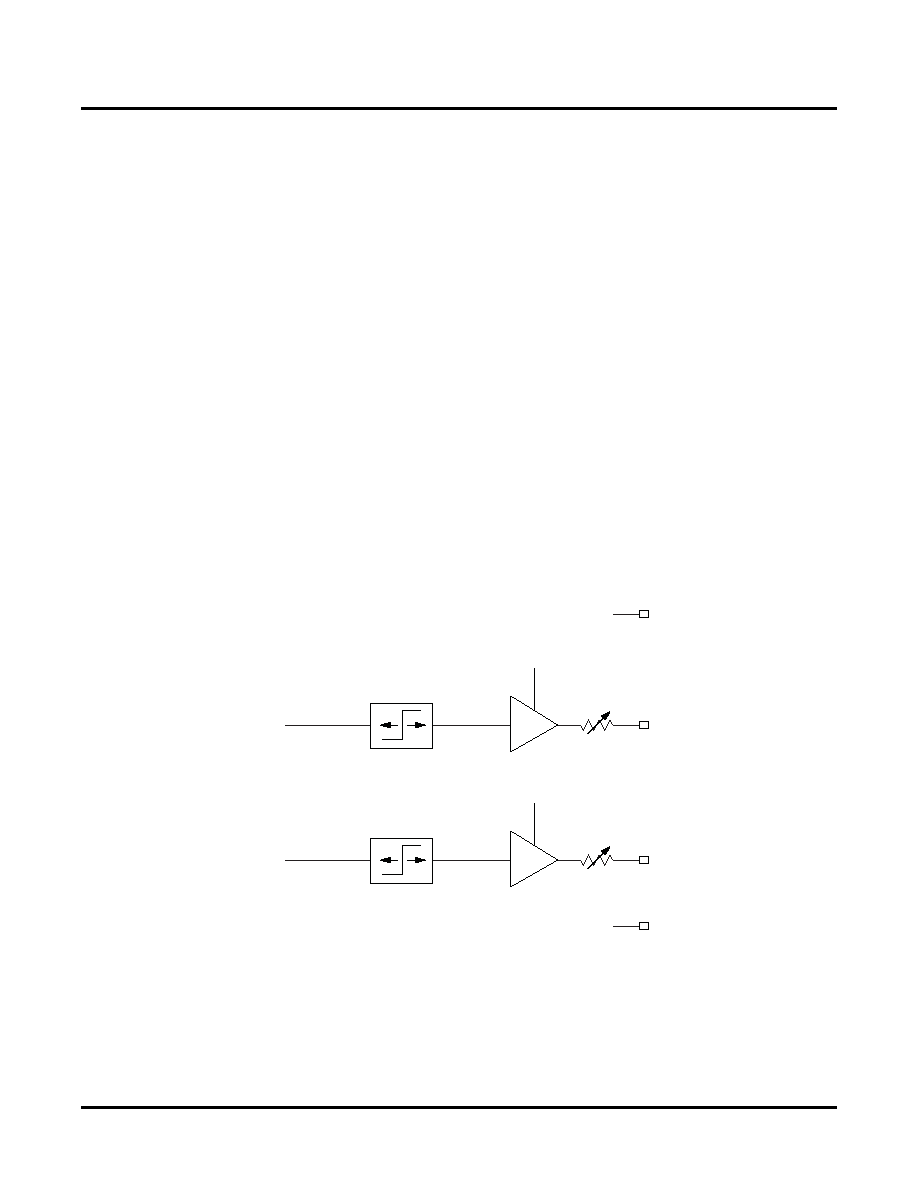
unequal PCB trace lengths or loading effects. Figure 19 shows a block diagram of a typical ispClock5300S output
driver bank and associated skew control.
Because of the high edge rates which can be generated by the ispClock5300S clock output drivers, the VCCO
power supply pin for each output bank should be individually bypassed. Low ESR capacitors with values ranging
from 0.01 to 0.1 F may be used for this purpose. Each bypass capacitor should be placed as close to its respec-
tive output bank power pins (VCCO and GNDO) pins as is possible to minimize interconnect length and associated
parasitic inductances.
In the case where an output bank is unused, the associated VCCO pin may be either left oating or tied to ground
to reduce quiescent power consumption. We recommend, however, that all unused VCCO pins be tied to ground
where possible. All GNDO pins must be tied to ground, regardless of whether or not the associated bank is used.
Figure 19. ispClock5300S Output Driver and Skew Control
*Skew Adjust Mechanism is applicable only to outputs connected to one of the three V-Dividers and
when PLL is active (PLL-Bypass pin = 0). For all other conditions, Skew Adjust Mechanism is bypassed.
OE Control
Bank_xA
Single Ended
Output A Driver
Skew
Adjust*
From
V-Dividers
OE Control
Bank_xB
Single Ended
Output B Driver
Skew
Adjust*
From
V-Dividers
GNDO-x
VCCO-x
相关PDF资料 |
PDF描述 |
|---|---|
| ISPPAC-CLK5312S-01TN48I | IC CLOCK PROGRAM BUFFER 48TQFP |
| VI-27Z-MX-F2 | CONVERTER MOD DC/DC 2V 30W |
| X9317TM8I-2.7T2 | IC XDCP 100TAP 100K 3WIRE 8-MSOP |
| X9314WST1 | IC XDCP SGL 32-TAP 10K 8-SOIC |
| ISPPAC-CLK5316S-01T64C | IC BUFFER FANOUT ISP UNIV 64TQFP |
相关代理商/技术参数 |
参数描述 |
|---|---|
| ISPPACCLK5312S-01T48I | 制造商:LATTICE 制造商全称:Lattice Semiconductor 功能描述:In-System Programmable, Zero-Delay, Universal Fan-Out Buffer, Single-Ended |
| ISPPACCLK5312S-01T64C | 制造商:LATTICE 制造商全称:Lattice Semiconductor 功能描述:In-System Programmable, Zero-Delay, Universal Fan-Out Buffer, Single-Ended |
| ISPPACCLK5312S-01T64I | 制造商:LATTICE 制造商全称:Lattice Semiconductor 功能描述:In-System Programmable, Zero-Delay, Universal Fan-Out Buffer, Single-Ended |
| ispPAC-CLK5312S-01TN48C | 功能描述:时钟驱动器及分配 ISP 0 Delay Unv Fan- Out Buf-Sngl End RoHS:否 制造商:Micrel 乘法/除法因子:1:4 输出类型:Differential 最大输出频率:4.2 GHz 电源电压-最大: 电源电压-最小:5 V 最大工作温度:+ 85 C 封装 / 箱体:SOIC-8 封装:Reel |
| ISPPACCLK5312S-01TN48C | 制造商:LATTICE 制造商全称:Lattice Semiconductor 功能描述:In-System Programmable, Zero-Delay, Universal Fan-Out Buffer, Single-Ended |
发布紧急采购,3分钟左右您将得到回复。