参数资料
| 型号: | KAD5612P-17Q72 |
| 厂商: | Intersil |
| 文件页数: | 7/29页 |
| 文件大小: | 0K |
| 描述: | IC ADC 12BIT 170MSPS DUAL 72-QFN |
| 产品培训模块: | High-Speed Analog-to-Digital Converters |
| 标准包装: | 1 |
| 系列: | FemtoCharge™ |
| 位数: | 12 |
| 采样率(每秒): | 170M |
| 数据接口: | 串行,SPI? |
| 转换器数目: | 2 |
| 功率耗散(最大): | 405mW |
| 电压电源: | 单电源 |
| 工作温度: | -40°C ~ 85°C |
| 安装类型: | 表面贴装 |
| 封装/外壳: | 72-VFQFN 裸露焊盘 |
| 供应商设备封装: | 72-QFN(10x10) |
| 包装: | 托盘 |
| 输入数目和类型: | 2 个差分,单极 |
第1页第2页第3页第4页第5页第6页当前第7页第8页第9页第10页第11页第12页第13页第14页第15页第16页第17页第18页第19页第20页第21页第22页第23页第24页第25页第26页第27页第28页第29页
15
FN6803.2
September 9, 2009
The calibration sequence is initiated on the rising edge of
RESETN, as shown in Figure 23. The over-range output
(OR) is set high once RESETN is pulled low, and remains in
that state until calibration is complete. The OR output returns
to normal operation at that time, so it is important that the
analog input be within the converter’s full-scale range to
observe the transition. If the input is in an over-range
condition the OR pin will stay high, and it will not be possible
to detect the end of the calibration cycle.
While RESETN is low, the output clock
(CLKOUTP/CLKOUTN) is set low. Normal operation of the
output clock resumes at the next input clock edge
(CLKP/CLKN) after RESETN is deasserted. At 250MSPS
the nominal calibration time is 200ms, while the maximum
calibration time is 550ms.
User-Initiated Reset
Recalibration of the ADC can be initiated at any time by
driving the RESETN pin low for a minimum of one clock
cycle. An open-drain driver with a drive strength of less than
0.5mA is recommended, RESETN has an internal high
impedance pull-up to OVDD. As is the case during power-on
reset, the SDO, RESETN and DNC pins must be in the
proper state for the calibration to successfully execute.
The performance of the KAD5612P changes with variations
in temperature, supply voltage or sample rate. The extent of
these changes may necessitate recalibration, depending on
system performance requirements. Best performance will be
achieved by recalibrating the ADC under the environmental
conditions at which it will operate.
A supply voltage variation of less than 100mV will generally
result in an SNR change of less than 0.5dBFS and SFDR
change of less than 3dBc.
In situations where the sample rate is not constant, best
results will be obtained if the device is calibrated at the
highest sample rate. Reducing the sample rate by less than
75MSPS will typically result in an SNR change of less than
0.5dBFS and an SFDR change of less than 3dBc.
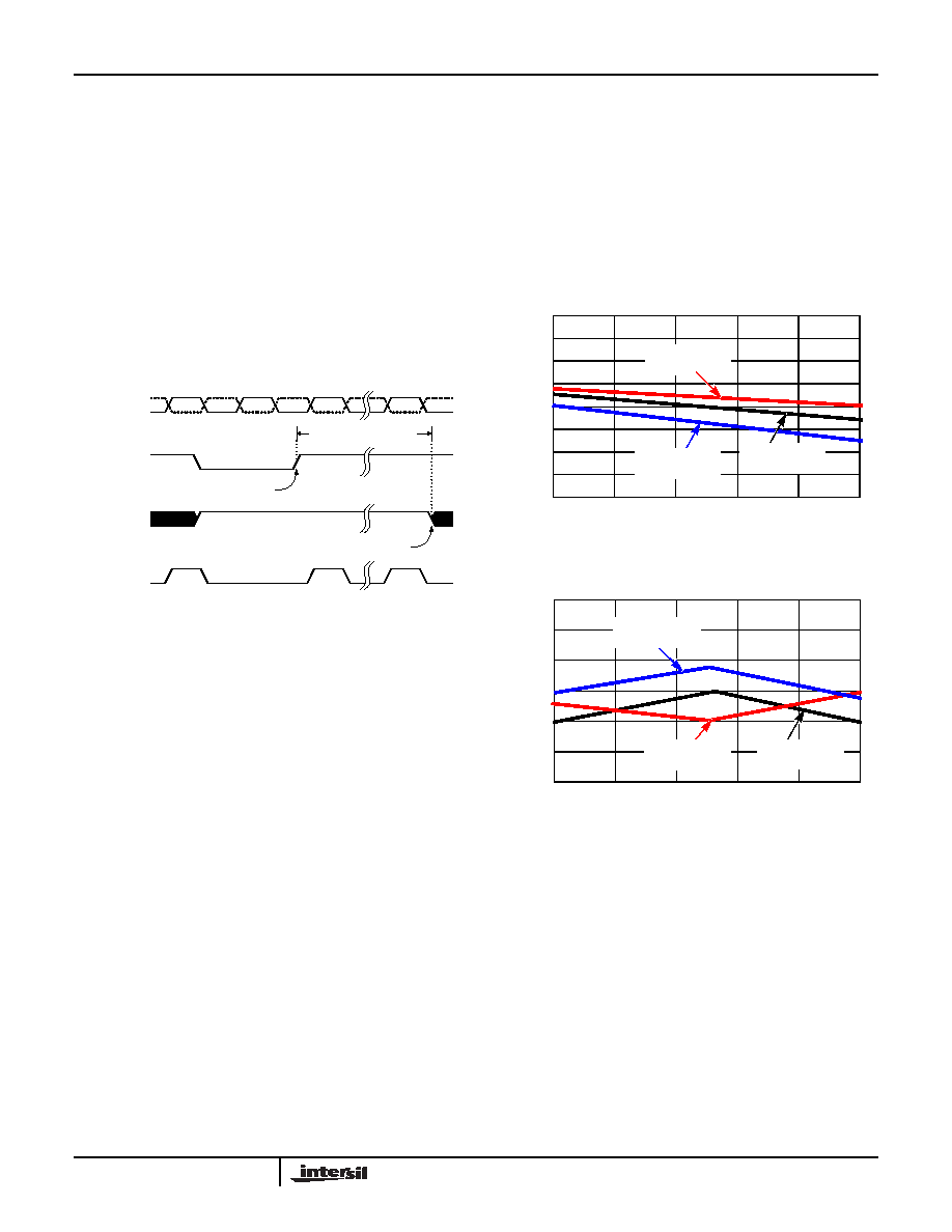
and SFDR performance with calibration performed at -40°C,
+25°C, and +85°C. Each plot shows the variation of
SNR/SFDR across temperature after a single calibration at
-40°C, +25°C and +85°C. Best performance is typically
achieved by a user-initiated calibration at the operating
conditions, as stated earlier. However, it can be seen that
performance drift with temperature is not a very strong
function of the temperature at which the calibration is
performed. Full-rated performance will be achieved after
power-up calibration regardless of the operating conditions.
Analog Input
Each ADC core contains a fully differential input
(AINP/AINN, BINP/BINN) to the sample and hold amplifier
(SHA). The ideal full-scale input voltage is 1.45V, centered at
the VCM voltage of 0.535V as shown in Figure 26.
Best performance is obtained when the analog inputs are
driven differentially. The common-mode output voltage,
VCM, should be used to properly bias the inputs as shown in
FIGURE 23. CALIBRATION TIMING
CLKP
CLKN
CLKOUTP
RESETN
ORP
CALIBRATION
BEGINS
CALIBRATION
COMPLETE
CALIBRATION
TIME
-4
-3
-2
-1
0
1
2
3
-40
-15
10
35
60
85
SNR
C
HANGE
(d
B
fs)
CAL DONE AT
+85°C
TEMPERATURE (°C)
CAL DONE AT
-40°C
CAL DONE AT
+25°C
FIGURE 24. SNR PERFORMANCE vs TEMPERATURE
FIGURE 25. SFDR PERFORMANCE vs TEMPERATURE
-15
-10
-5
0
5
10
15
-40
-15
10
35
60
85
SFDR
CHANGE
(dBc)
TEMPERATURE (°C)
CAL DONE AT
-40°C
CAL DONE AT
+25°C
CAL DONE AT
+85°C
KAD5612P
相关PDF资料 |
PDF描述 |
|---|---|
| LA72715NV-TLM-E | IC AUDIO DECODER JPN MTS 24SSOP |
| LICAL-DEC-LS001 | IC DECODER LOW SECURITY 8DIP |
| LICAL-DEC-MS001 | IC DECODER MS SERIES 20-SSOP |
| LICAL-ENC-MS001 | IC ENCODER MS SERIES 20-SSOP |
| LICAL-TRC-MT | IC TRANSCODER MT BI-DIR 20-SSOP |
相关代理商/技术参数 |
参数描述 |
|---|---|
| KAD5612P-21Q72 | 制造商:Intersil Corporation 功能描述:ADC DUAL PIPELINED 210MSPS 12-BIT PARALLEL 72QFN EP - Rail/Tube 制造商:Intersil Corporation 功能描述:IC ADC 12BIT 210MSPS DUAL 72-QFN 制造商:Intersil Corporation 功能描述:12-Bit, 210MSPS Dual-Channel ADC, Programmable LVDS/LVCMOS Outputs. 72- QFN 制造商:Intersil Corporation 功能描述:KAD5612P Series Dual Ch 12-Bit SMT Analog to Digital Converter QFN-72EP 制造商:Intersil Corporation 功能描述:Analog to Digital Converters - ADC 12-BIT 210MSPS DL-CH ADC PROG LVDS/LVCMOS |
| KAD5612P-25Q72 | 制造商:Intersil Corporation 功能描述:ADC DUAL PIPELINED 250MSPS 12-BIT PARALLEL 72QFN EP - Rail/Tube 制造商:Intersil Corporation 功能描述:IC ADC 12BIT 250MSPS DUAL 72-QFN 制造商:Intersil Corporation 功能描述:IC, ADC, 12BIT, Resolution (Bits):12bit, Sampling Rate:250MSPS, Supply Voltage T |
| KA-D9E-011 | 制造商:Leach International Corporation 功能描述:MID RANGE - Bulk |
| KA-D9F-005 | 制造商:Leach International Corporation 功能描述:MID RANGE - Bulk |
| KA-D9F-010 | 制造商:Leach International Corporation 功能描述:MDAC DC-10,MD-11 AIR LINE - Bulk |
发布紧急采购,3分钟左右您将得到回复。