- 您现在的位置:买卖IC网 > PDF目录299258 > KFM4GH6Q4M-DEB80 256M X 16 FLASH 1.8V PROM, 70 ns, PBGA63 PDF资料下载
参数资料
| 型号: | KFM4GH6Q4M-DEB80 |
| 元件分类: | PROM |
| 英文描述: | 256M X 16 FLASH 1.8V PROM, 70 ns, PBGA63 |
| 封装: | 10 X 13 MM, 1 MM HEIGHT, 0.80 MM PITCH, LEAD FREE, FBGA-63 |
| 文件页数: | 2/142页 |
| 文件大小: | 2226K |
| 代理商: | KFM4GH6Q4M-DEB80 |
第1页当前第2页第3页第4页第5页第6页第7页第8页第9页第10页第11页第12页第13页第14页第15页第16页第17页第18页第19页第20页第21页第22页第23页第24页第25页第26页第27页第28页第29页第30页第31页第32页第33页第34页第35页第36页第37页第38页第39页第40页第41页第42页第43页第44页第45页第46页第47页第48页第49页第50页第51页第52页第53页第54页第55页第56页第57页第58页第59页第60页第61页第62页第63页第64页第65页第66页第67页第68页第69页第70页第71页第72页第73页第74页第75页第76页第77页第78页第79页第80页第81页第82页第83页第84页第85页第86页第87页第88页第89页第90页第91页第92页第93页第94页第95页第96页第97页第98页第99页第100页第101页第102页第103页第104页第105页第106页第107页第108页第109页第110页第111页第112页第113页第114页第115页第116页第117页第118页第119页第120页第121页第122页第123页第124页第125页第126页第127页第128页第129页第130页第131页第132页第133页第134页第135页第136页第137页第138页第139页第140页第141页第142页
Flex-MuxOneNAND4G(KFM4GH6Q4M-DEBx)
- 10 -
FLASH MEMORY
Flex-MuxOneNAND8G(KFN8GH6Q4M-DEBx)
Flex-MuxOneNAND16G(KFKAGH6Q4M-DEBx)
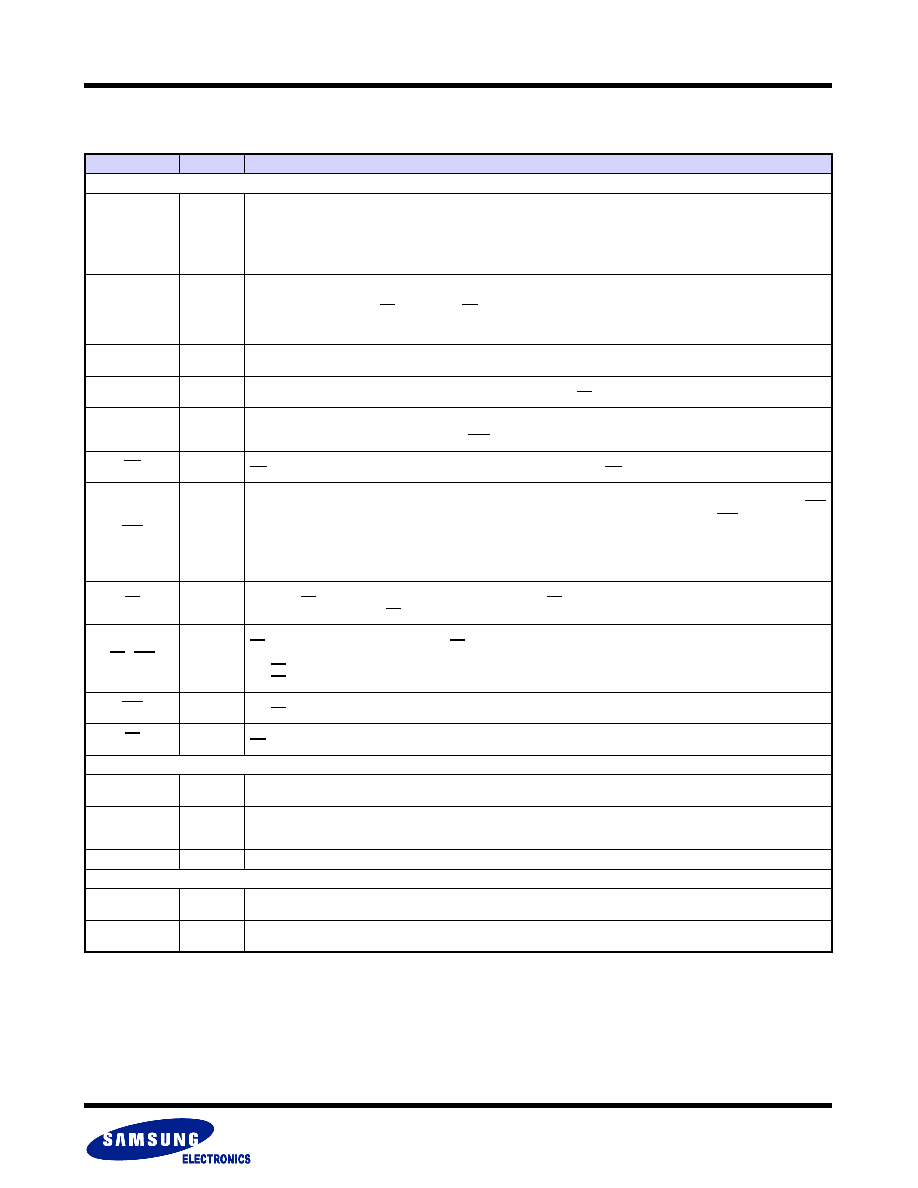
2.4 Pin Description
NOTE :
Do not leave power supply(Vcc-Core/Vcc-IO, VSS) disconnected.
Pin Name
Type
Nameand Description
Host Interface
ADQ15~ADQ0
I/O
Multiplexed Address/Data bus
- Inputs for addresses during read operation, which are for addressing BufferRAM & Register.
- Inputs data during program and commands for all operations, outputs data during memory array/
register read cycles.
Data pins float to high-impedance when the chip is deselected or outputs are disabled.
INT / INT1
O
Interrupt
Notifies the Host when a command is completed. After power-up, it is at hi-z condition. Once IOBE is set to 1, it does not float
to hi-z condition even when CE is disabled or OE is disabled. Especially, only when reset(Cold, Warm, Hot, NAND Flash
Core) command in DDP are issued, it operates as open drain output with internal resistor (~50Kohm). The INT is the interrupt
for Single or DDP device. The INT1 is the interrupt for the first DDP device(KFN8GH6Q4M) in QDP(KFKAGH6Q4M)
INT2
O
Interrupt
The INT2 is the interrupt for the second DDP device(KFN8GH6Q4M) in QDP(KFKAGH6Q4M)
RDY
O
Ready
Indicates data valid in synchronous read modes and is activated while CE is low
CLK
I
Clock
CLK synchronizes the device to the system bus frequency in synchronous read mode.
The first rising edge of CLK in conjunction with AVD low latches address input.
WE
I
Write Enable
WE controls writes to the bufferRAM and registers. Datas are latched on the WE pulse’s rising edge
AVD
I
Address Valid Detect
Indicates valid address presence on address inputs. During asynchronous read operation, all addresses are valid while AVD
is low, and during synchronous read operation, all addresses are latched on CLK’s rising edge while AVD is held low for one
clock cycle.
> Low : for asynchronous mode, indicates valid address; for burst mode, causes starting address to be latched on rising edge
on CLK
> High : device ignores address inputs
RP
I
Reset Pin
When low, RP resets internal operation of Flex-MuxOneNAND. RP status is do not care during power-up
and bootloading. When high, RP level must be equivalent to Vcc-IO / Vccq level.
CE / CE1
I
Chip Enable
CE-low activates internal control logic, and CE-high deselects the device, places it in standby state,
and places DQ in Hi-Z.
The CE input enables device for Single or DDP .
The CE1 input enables the first DDP device(KFN8GH6Q4M) in QDP(KFKAGH6Q4M)
CE2
I
Chip Enable
The CE2 input enables the second DDP device(KFN8GH6Q4M) in QDP(KFKAGH6Q4M)
OE
I
Output Enable
OE-low enables the device’s output data buffers during a read cycle.
Power Supply
VCC-Core
/ Vcc
Power for Flex-MuxOneNAND Core
This is the power supply for Flex-MuxOneNAND Core.
VCC-IO
/ Vccq
Power for Flex-MuxOneNAND I/O
This is the power supply for Flex-MuxOneNAND I/O
Vcc-IO / Vccq is internally separated from Vcc-Core / Vcc.
VSS
Ground for Flex-MuxOneNAND
etc.
DNU
Do Not Use
Leave it disconnected. These pins are used for testing.
NC
No Connection
Lead is not internally connected.
相关PDF资料 |
PDF描述 |
|---|---|
| KHP7 | 2.75 A, 7000 V, SILICON, RECTIFIER DIODE |
| KJA1Y13K8PC | 8 CONTACT(S), STEEL, MALE, MIL SERIES CONNECTOR, SOLDER, RECEPTACLE |
| KJA1Y13K8PD | 8 CONTACT(S), STEEL, MALE, MIL SERIES CONNECTOR, SOLDER, RECEPTACLE |
| KJA1Y13K8PE | 8 CONTACT(S), STEEL, MALE, MIL SERIES CONNECTOR, SOLDER, RECEPTACLE |
| KJA1Y13K8PN | 8 CONTACT(S), STEEL, MALE, MIL SERIES CONNECTOR, SOLDER, RECEPTACLE |
相关代理商/技术参数 |
参数描述 |
|---|---|
| KFM65MZ-160PR | 制造商:TYAN 功能描述:CHASSIS UNIT - Bulk |
| KFM85M | 制造商:KEC 制造商全称:KEC(Korea Electronics) 功能描述:SPECIFICATIONS FOR SAW FILTER(BAND PASS FILTERS FOR CDMA IF STAGE) |
| KFM90D060 | 制造商:IDEC CORPORATION 功能描述:CONNECTOR M12 |
| KFM90D060R | 制造商:IDEC CORPORATION 功能描述:CONNECTOR M12 |
| KFM90D150 | 制造商:IDEC CORPORATION 功能描述:CONNECTOR M12 |
发布紧急采购,3分钟左右您将得到回复。