- 您现在的位置:买卖IC网 > PDF目录22053 > KMC8144SVT1000B (Freescale Semiconductor)IC DSP 783FCPBGA PDF资料下载
参数资料
| 型号: | KMC8144SVT1000B |
| 厂商: | Freescale Semiconductor |
| 文件页数: | 50/80页 |
| 文件大小: | 0K |
| 描述: | IC DSP 783FCPBGA |
| 标准包装: | 2 |
| 系列: | StarCore |
| 类型: | SC3400 内核 |
| 接口: | EBI/EMI,以太网,I²C,PCI,Serial RapidIO,SPI,TDM,UART,UTOPIA |
| 时钟速率: | 1.0GHz |
| 非易失内存: | ROM(96 kB) |
| 芯片上RAM: | 10.5MB |
| 电压 - 输入/输出: | 3.30V |
| 电压 - 核心: | 1.00V |
| 工作温度: | 0°C ~ 105°C |
| 安装类型: | 表面贴装 |
| 封装/外壳: | 783-BBGA,FCBGA |
| 供应商设备封装: | 783-FCPBGA(29x29) |
| 包装: | 托盘 |
第1页第2页第3页第4页第5页第6页第7页第8页第9页第10页第11页第12页第13页第14页第15页第16页第17页第18页第19页第20页第21页第22页第23页第24页第25页第26页第27页第28页第29页第30页第31页第32页第33页第34页第35页第36页第37页第38页第39页第40页第41页第42页第43页第44页第45页第46页第47页第48页第49页当前第50页第51页第52页第53页第54页第55页第56页第57页第58页第59页第60页第61页第62页第63页第64页第65页第66页第67页第68页第69页第70页第71页第72页第73页第74页第75页第76页第77页第78页第79页第80页
�� �
�
�Electrical� Characteristics�
�2.6.5.8�
�Eye� Template� Measurements�
�For� the� purpose� of� eye� template� measurements,� the� effects� of� a� single-pole� high� pass� filter� with� a� 3� dB� point� at� (baud�
�frequency)/1667� is� applied� to� the� jitter.� The� data� pattern� for� template� measurements� is� the� continuous� jitter� test� pattern� (CJPAT)�
�defined� in� Annex� 48A� of� IEEE� Std.� 802.3ae.� All� lanes� of� the� LP-Serial� link� shall� be� active� in� both� the� transmit� and� receive�
�directions,� and� opposite� ends� of� the� links� shall� use� asynchronous� clocks.� Four� lane� implementations� shall� use� CJPAT� as� defined�
�in� Annex� 48A.� Single� lane� implementations� shall� use� the� CJPAT� sequence� specified� in� Annex� 48A� for� transmission� on� lane� 0.�
�The� amount� of� data� represented� in� the� eye� shall� be� adequate� to� ensure� that� the� bit� error� ratio� is� less� than� 10� –12� .� The� eye� pattern�
�shall� be� measured� with� AC� coupling� and� the� compliance� template� centered� at� 0� Volts� differential.� The� left� and� right� edges� of�
�the� template� shall� be� aligned� with� the� mean� zero� crossing� points� of� the� measured� data� eye.� The� load� for� this� test� shall� be� 100� Ω�
�resistive� ±� 5%� differential� to� 2.5� GHz.�
�2.6.5.9�
�Jitter� Test� Measurements�
�For� the� purpose� of� jitter� measurement,� the� effects� of� a� single-pole� high� pass� filter� with� a� 3� dB� point� at� (baud� frequency)/1667� is�
�applied� to� the� jitter.� The� data� pattern� for� jitter� measurements� is� the� Continuous� Jitter� Test� Pattern� (CJPAT)� pattern� defined� in�
�Annex� 48A� of� IEEE� Std.� 802.3ae.� All� lanes� of� the� LP-Serial� link� shall� be� active� in� both� the� transmit� and� receive� directions,� and�
�opposite� ends� of� the� links� shall� use� asynchronous� clocks.� Four� lane� implementations� shall� use� CJPAT� as� defined� in� Annex� 48A.�
�Single� lane� implementations� shall� use� the� CJPAT� sequence� specified� in� Annex� 48A� for� transmission� on� lane� 0.� Jitter� shall� be�
�measured� with� AC� coupling� and� at� 0� V� differential.� Jitter� measurement� for� the� transmitter� (or� for� calibration� of� a� jitter� tolerance�
�setup)� shall� be� performed� with� a� test� procedure� resulting� in� a� BER� curve� such� as� that� described� in� Annex� 48B� of� IEEE� Std.�
�802.3ae.�
�2.6.5.10�
�Transmit� Jitter�
�Transmit� jitter� is� measured� at� the� driver� output� when� terminated� into� a� load� of� 100� Ω� resistive� ±� 5%� differential� to� 2.5� GHz.�
�2.6.5.11�
�Jitter� Tolerance�
�Jitter� tolerance� is� measured� at� the� receiver� using� a� jitter� tolerance� test� signal.� This� signal� is� obtained� by� first� producing� the� sum�
�of� deterministic� and� random� jitter� defined� in� Section� 2.6.5.9� and� then� adjusting� the� signal� amplitude� until� the� data� eye� contacts�
�the� 6� points� of� the� minimum� eye� opening� of� the� receive� template� shown� in� Figure� 14� and� Table� 35� .� Note� that� for� this� to� occur,�
�the� test� signal� must� have� vertical� waveform� symmetry� about� the� average� value� and� have� horizontal� symmetry� (including� jitter)�
�about� the� mean� zero� crossing.� Eye� template� measurement� requirements� are� as� defined� above.� Random� jitter� is� calibrated� using�
�a� high� pass� filter� with� a� low� frequency� corner� at� 20� MHz� and� a� 20� dB/decade� roll-off� below� this.� The� required� sinusoidal� jitter�
�specified� in� Section� 8.6� is� then� added� to� the� signal� and� the� test� load� is� replaced� by� the� receiver� being� tested.�
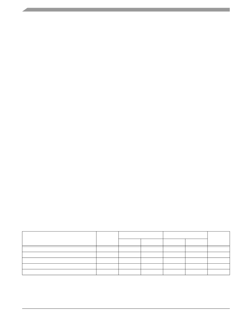
�2.6.6�
�PCI� Timing�
�This� section� describes� the� general� AC� timing� parameters� of� the� PCI� bus.� Table� 36� provides� the� PCI� AC� timing� specifications.�
�Table� 36.� PCI� AC� Timing� Specifications�
�33� MHz�
�66� MHz�
�Parameter�
�Symbol�
�Unit�
�Min�
�Max�
�Min�
�Max�
�Output� delay�
�High-Z� to� Valid� Output� delay�
�Valid� to� High-Z� Output� delay�
�Input� setup�
�Input� hold�
�t� PCVAL�
�t� PCON�
�t� PCOFF�
�t� PCSU�
�t� PCH�
�2.0�
�2.0�
�—�
�7.0�
�0�
�11.0�
�—�
�28�
�—�
�—�
�1.0�
�1.0�
�—�
�3.0�
�0�
�6.0�
�—�
�14�
�—�
�—�
�ns�
�ns�
�ns�
�ns�
�ns�
�MSC8144� Quad� Core� Digital� Signal� Processor� Data� Sheet,� Rev.� 16�
�50�
�Freescale� Semiconductor�
�相关PDF资料 |
PDF描述 |
|---|---|
| KMC8144VT800B | IC DSP 783FCPBGA |
| TAJC686K010ANJ | CAP TANT 68UF 10V 10% 2312 |
| KMC8144VT800A | IC DSP 783FCPBGA |
| KMC8144VT1000B | IC DSP 783FCPBGA |
| GEC10DRTN-S734 | CONN EDGECARD 20POS DIP .100 SLD |
相关代理商/技术参数 |
参数描述 |
|---|---|
| KMC8144SVT800A | 功能描述:数字信号处理器和控制器 - DSP, DSC PACSUN SAMPLE PART RoHS:否 制造商:Microchip Technology 核心:dsPIC 数据总线宽度:16 bit 程序存储器大小:16 KB 数据 RAM 大小:2 KB 最大时钟频率:40 MHz 可编程输入/输出端数量:35 定时器数量:3 设备每秒兆指令数:50 MIPs 工作电源电压:3.3 V 最大工作温度:+ 85 C 封装 / 箱体:TQFP-44 安装风格:SMD/SMT |
| KMC8144SVT800B | 功能描述:IC DSP 783FCPBGA RoHS:是 类别:集成电路 (IC) >> 嵌入式 - DSP(数字式信号处理器) 系列:StarCore 标准包装:40 系列:TMS320DM64x, DaVinci™ 类型:定点 接口:I²C,McASP,McBSP 时钟速率:400MHz 非易失内存:外部 芯片上RAM:160kB 电压 - 输入/输出:3.30V 电压 - 核心:1.20V 工作温度:0°C ~ 90°C 安装类型:表面贴装 封装/外壳:548-BBGA,FCBGA 供应商设备封装:548-FCBGA(27x27) 包装:托盘 配用:TMDSDMK642-0E-ND - DEVELPER KIT W/NTSC CAMERA296-23038-ND - DSP STARTER KIT FOR TMS320C6416296-23059-ND - FLASHBURN PORTING KIT296-23058-ND - EVAL MODULE FOR DM642TMDSDMK642-ND - DEVELOPER KIT W/NTSC CAMERA |
| KMC8144TVT1000A | 功能描述:数字信号处理器和控制器 - DSP, DSC PACSUN SAMPLE PART RoHS:否 制造商:Microchip Technology 核心:dsPIC 数据总线宽度:16 bit 程序存储器大小:16 KB 数据 RAM 大小:2 KB 最大时钟频率:40 MHz 可编程输入/输出端数量:35 定时器数量:3 设备每秒兆指令数:50 MIPs 工作电源电压:3.3 V 最大工作温度:+ 85 C 封装 / 箱体:TQFP-44 安装风格:SMD/SMT |
| KMC8144TVT1000B | 功能描述:IC DSP 783FCPBGA RoHS:是 类别:集成电路 (IC) >> 嵌入式 - DSP(数字式信号处理器) 系列:StarCore 标准包装:40 系列:TMS320DM64x, DaVinci™ 类型:定点 接口:I²C,McASP,McBSP 时钟速率:400MHz 非易失内存:外部 芯片上RAM:160kB 电压 - 输入/输出:3.30V 电压 - 核心:1.20V 工作温度:0°C ~ 90°C 安装类型:表面贴装 封装/外壳:548-BBGA,FCBGA 供应商设备封装:548-FCBGA(27x27) 包装:托盘 配用:TMDSDMK642-0E-ND - DEVELPER KIT W/NTSC CAMERA296-23038-ND - DSP STARTER KIT FOR TMS320C6416296-23059-ND - FLASHBURN PORTING KIT296-23058-ND - EVAL MODULE FOR DM642TMDSDMK642-ND - DEVELOPER KIT W/NTSC CAMERA |
| KMC8144TVT800A | 功能描述:数字信号处理器和控制器 - DSP, DSC PACSUN SAMPLE PART RoHS:否 制造商:Microchip Technology 核心:dsPIC 数据总线宽度:16 bit 程序存储器大小:16 KB 数据 RAM 大小:2 KB 最大时钟频率:40 MHz 可编程输入/输出端数量:35 定时器数量:3 设备每秒兆指令数:50 MIPs 工作电源电压:3.3 V 最大工作温度:+ 85 C 封装 / 箱体:TQFP-44 安装风格:SMD/SMT |
发布紧急采购,3分钟左右您将得到回复。