- 您现在的位置:买卖IC网 > PDF目录3944 > KMPC8544EAVTANG (Freescale Semiconductor)IC MPU POWERQUICC III 783-PBGA PDF资料下载
参数资料
| 型号: | KMPC8544EAVTANG |
| 厂商: | Freescale Semiconductor |
| 文件页数: | 25/117页 |
| 文件大小: | 0K |
| 描述: | IC MPU POWERQUICC III 783-PBGA |
| 标准包装: | 2 |
| 系列: | MPC85xx |
| 处理器类型: | 32-位 MPC85xx PowerQUICC III |
| 速度: | 800MHz |
| 电压: | 1V |
| 安装类型: | 表面贴装 |
| 封装/外壳: | 783-BBGA,FCBGA |
| 供应商设备封装: | 783-FCPBGA(29x29) |
| 包装: | 托盘 |
第1页第2页第3页第4页第5页第6页第7页第8页第9页第10页第11页第12页第13页第14页第15页第16页第17页第18页第19页第20页第21页第22页第23页第24页当前第25页第26页第27页第28页第29页第30页第31页第32页第33页第34页第35页第36页第37页第38页第39页第40页第41页第42页第43页第44页第45页第46页第47页第48页第49页第50页第51页第52页第53页第54页第55页第56页第57页第58页第59页第60页第61页第62页第63页第64页第65页第66页第67页第68页第69页第70页第71页第72页第73页第74页第75页第76页第77页第78页第79页第80页第81页第82页第83页第84页第85页第86页第87页第88页第89页第90页第91页第92页第93页第94页第95页第96页第97页第98页第99页第100页第101页第102页第103页第104页第105页第106页第107页第108页第109页第110页第111页第112页第113页第114页第115页第116页第117页
MPC8544E PowerQUICC III Integrated Processor Hardware Specifications, Rev. 6
Freescale Semiconductor
15
Input Clocks
4.2
Real-Time Clock Timing
The RTC input is sampled by the platform clock (CCB clock). The output of the sampling latch is then
used as an input to the counters of the PIC and the TimeBase unit of the e500. There is no jitter
specification. The minimum pulse width of the RTC signal should be greater than 2 × the period of the
CCB clock. That is, minimum clock high time is 2
× t
CCB, and minimum clock low time is 2 × tCCB. There
is no minimum RTC frequency; RTC may be grounded if not needed.
4.3
eTSEC Gigabit Reference Clock Timing
Table 7 provides the eTSEC gigabit reference clocks (EC_GTX_CLK125) AC timing specifications for
the MPC8544E.
4.4
Platform to FIFO Restrictions
Please note the following FIFO maximum speed restrictions based on platform speed.
For FIFO GMII mode:
FIFO TX/RX clock frequency
≤platform clock frequency ÷ 4.2
For example, if the platform frequency is 533 MHz, the FIFO Tx/Rx clock frequency should be no more
than 127 MHz.
For FIFO encoded mode:
FIFO TX/RX clock frequency
≤platform clock frequency ÷ 3.2
For example, if the platform frequency is 533 MHz, the FIFO Tx/Rx clock frequency should be no more
than 167 MHz.
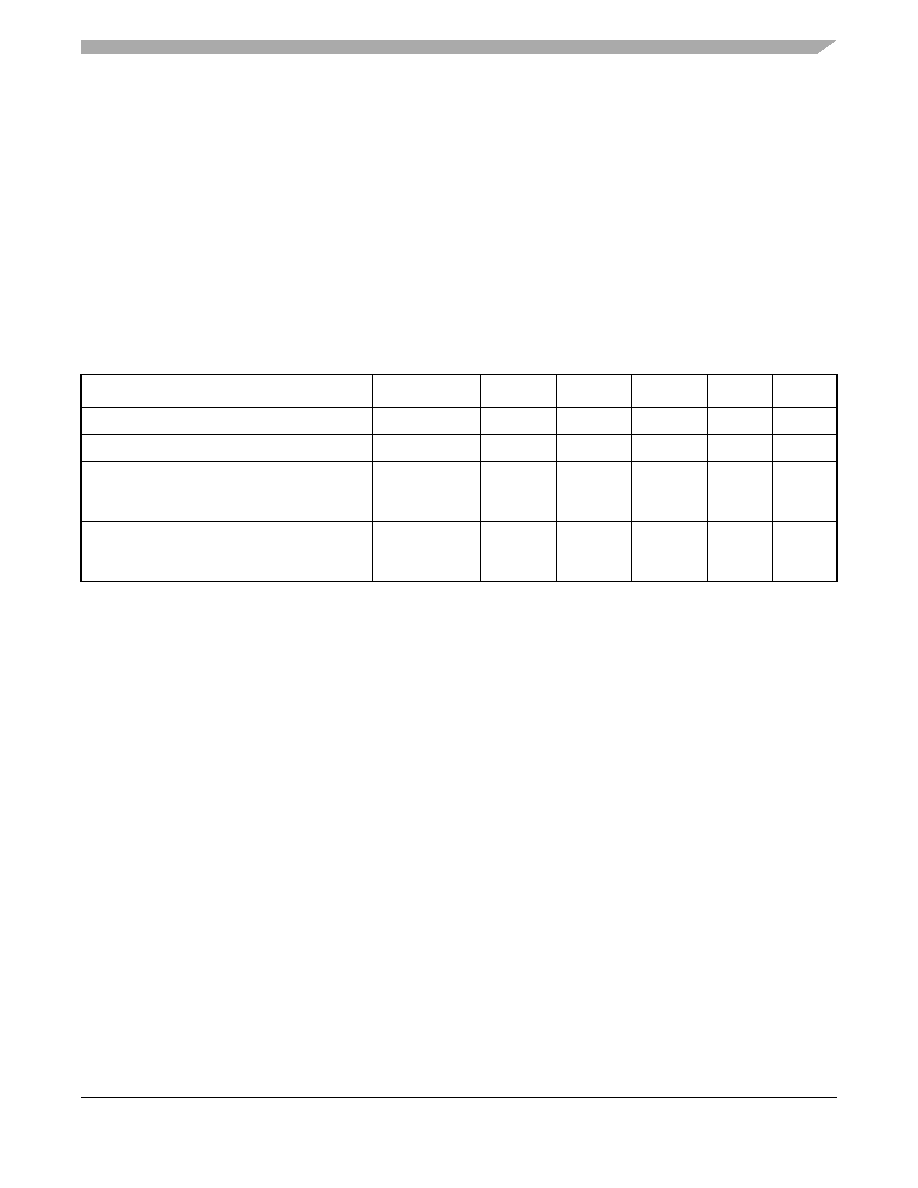
Table 7. EC_GTX_CLK125 AC Timing Specifications
Parameter/Condition
Symbol
Min
Typ
Max
Unit
Notes
EC_GTX_CLK125 frequency
fG125
—125
—
MHz
—
EC_GTX_CLK125 cycle time
tG125
—8—
ns
—
EC_GTX_CLK rise and fall time
LVDD, TVDD = 2.5 V
LVDD, TVDD = 3.3 V
tG125R/tG125F
——
0.75
1.0
ns
1
EC_GTX_CLK125 duty cycle
GMII, TBI
1000Base-T for RGMII, RTBI
tG125H/tG125
45
47
—
55
53
%2
Notes:
1. Rise and fall times for EC_GTX_CLK125 are measured from 0.5 and 2.0 V for L/TVDD = 2.5 V, and from 0.6 and 2.7 V for
L/TVDD = 3.3 V.
2. EC_GTX_CLK125 is used to generate the GTX clock for the eTSEC transmitter with 2% degradation. EC_GTX_CLK125 duty
cycle can be loosened from 47%/53% as long as the PHY device can tolerate the duty cycle generated by the eTSEC
GTX_CLK. See Section 8.7.4, “RGMII and RTBI AC Timing Specifications,” for duty cycle for 10Base-T and 100Base-T
reference clock.
相关PDF资料 |
PDF描述 |
|---|---|
| 345-012-521-202 | CARDEDGE 12POS DUAL .100 GREEN |
| IDT70V5388S200BCG | IC SRAM 1.125MBIT 200MHZ 256BGA |
| KMPC8533EVTAQG | IC MPU POWERQUICC III 783-PBGA |
| 345-012-521-201 | CARDEDGE 12POS DUAL .100 GREEN |
| 395-010-541-202 | CARD EDGE 10POS DL .100X.200 BLK |
相关代理商/技术参数 |
参数描述 |
|---|---|
| KMPC8544EAVTAQG | 功能描述:微处理器 - MPU PQ38K 8544E COMMERCIAL RoHS:否 制造商:Atmel 处理器系列:SAMA5D31 核心:ARM Cortex A5 数据总线宽度:32 bit 最大时钟频率:536 MHz 程序存储器大小:32 KB 数据 RAM 大小:128 KB 接口类型:CAN, Ethernet, LIN, SPI,TWI, UART, USB 工作电源电压:1.8 V to 3.3 V 最大工作温度:+ 85 C 安装风格:SMD/SMT 封装 / 箱体:FBGA-324 |
| KMPC8544EVTANG | 功能描述:微处理器 - MPU PQ38K 8544E RoHS:否 制造商:Atmel 处理器系列:SAMA5D31 核心:ARM Cortex A5 数据总线宽度:32 bit 最大时钟频率:536 MHz 程序存储器大小:32 KB 数据 RAM 大小:128 KB 接口类型:CAN, Ethernet, LIN, SPI,TWI, UART, USB 工作电源电压:1.8 V to 3.3 V 最大工作温度:+ 85 C 安装风格:SMD/SMT 封装 / 箱体:FBGA-324 |
| KMPC8544EVTAQG | 功能描述:微处理器 - MPU PQ38K 8544E RoHS:否 制造商:Atmel 处理器系列:SAMA5D31 核心:ARM Cortex A5 数据总线宽度:32 bit 最大时钟频率:536 MHz 程序存储器大小:32 KB 数据 RAM 大小:128 KB 接口类型:CAN, Ethernet, LIN, SPI,TWI, UART, USB 工作电源电压:1.8 V to 3.3 V 最大工作温度:+ 85 C 安装风格:SMD/SMT 封装 / 箱体:FBGA-324 |
| KMPC8545EHXANG | 功能描述:微处理器 - MPU PQ38 8548E RoHS:否 制造商:Atmel 处理器系列:SAMA5D31 核心:ARM Cortex A5 数据总线宽度:32 bit 最大时钟频率:536 MHz 程序存储器大小:32 KB 数据 RAM 大小:128 KB 接口类型:CAN, Ethernet, LIN, SPI,TWI, UART, USB 工作电源电压:1.8 V to 3.3 V 最大工作温度:+ 85 C 安装风格:SMD/SMT 封装 / 箱体:FBGA-324 |
| KMPC8545EHXAQG | 功能描述:微处理器 - MPU PQ38 8548E RoHS:否 制造商:Atmel 处理器系列:SAMA5D31 核心:ARM Cortex A5 数据总线宽度:32 bit 最大时钟频率:536 MHz 程序存储器大小:32 KB 数据 RAM 大小:128 KB 接口类型:CAN, Ethernet, LIN, SPI,TWI, UART, USB 工作电源电压:1.8 V to 3.3 V 最大工作温度:+ 85 C 安装风格:SMD/SMT 封装 / 箱体:FBGA-324 |
发布紧急采购,3分钟左右您将得到回复。