- 您现在的位置:买卖IC网 > PDF目录3944 > KMPC8544EAVTANG (Freescale Semiconductor)IC MPU POWERQUICC III 783-PBGA PDF资料下载
参数资料
| 型号: | KMPC8544EAVTANG |
| 厂商: | Freescale Semiconductor |
| 文件页数: | 42/117页 |
| 文件大小: | 0K |
| 描述: | IC MPU POWERQUICC III 783-PBGA |
| 标准包装: | 2 |
| 系列: | MPC85xx |
| 处理器类型: | 32-位 MPC85xx PowerQUICC III |
| 速度: | 800MHz |
| 电压: | 1V |
| 安装类型: | 表面贴装 |
| 封装/外壳: | 783-BBGA,FCBGA |
| 供应商设备封装: | 783-FCPBGA(29x29) |
| 包装: | 托盘 |
第1页第2页第3页第4页第5页第6页第7页第8页第9页第10页第11页第12页第13页第14页第15页第16页第17页第18页第19页第20页第21页第22页第23页第24页第25页第26页第27页第28页第29页第30页第31页第32页第33页第34页第35页第36页第37页第38页第39页第40页第41页当前第42页第43页第44页第45页第46页第47页第48页第49页第50页第51页第52页第53页第54页第55页第56页第57页第58页第59页第60页第61页第62页第63页第64页第65页第66页第67页第68页第69页第70页第71页第72页第73页第74页第75页第76页第77页第78页第79页第80页第81页第82页第83页第84页第85页第86页第87页第88页第89页第90页第91页第92页第93页第94页第95页第96页第97页第98页第99页第100页第101页第102页第103页第104页第105页第106页第107页第108页第109页第110页第111页第112页第113页第114页第115页第116页第117页
MPC8544E PowerQUICC III Integrated Processor Hardware Specifications, Rev. 6
30
Freescale Semiconductor
Enhanced Three-Speed Ethernet (eTSEC), MII Management
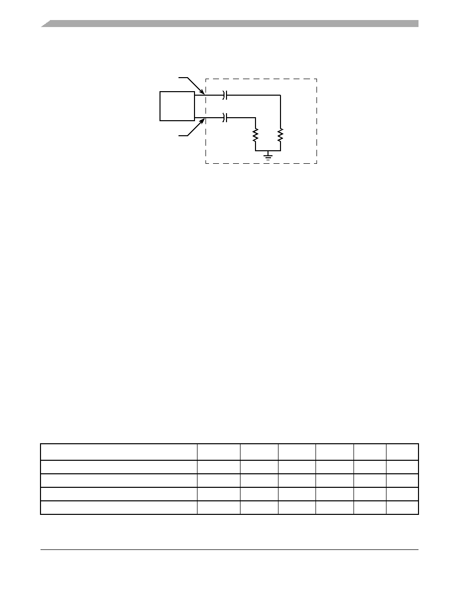
Figure 10 provides the AC test load for SGMII.
Figure 10. SGMII AC Test/Measurement Load
8.5
FIFO, GMII,MII, TBI, RGMII, RMII, and RTBI AC Timing
Specifications
The AC timing specifications for FIFO, GMII, MII, TBI, RGMII, RMII, and RTBI are presented in this
section.
8.5.1
FIFO AC Specifications
The basis for the AC specifications for the eTSEC FIFO modes is the double data rate RGMII and RTBI
specifications, since they have similar performance and are described in a source-synchronous fashion like
FIFO modes. However, the FIFO interface provides deliberate skew between the transmitted data and
source clock in GMII fashion.
When the eTSEC is configured for FIFO modes, all clocks are supplied from external sources to the
relevant eTSEC interface. That is, the transmit clock must be applied to the eTSECn TSECn_TX_CLK,
while the receive clock must be applied to pin TSECn_RX_CLK. The eTSEC internally uses the transmit
clock to synchronously generate transmit data and outputs an echoed copy of the transmit clock back out
onto the TSECn_GTX_CLK pin (while transmit data appears on TSECn_TXD[7:0], for example). It is
intended that external receivers capture eTSEC transmit data using the clock on TSECn_GTX_CLK as a
source-synchronous timing reference. Typically, the clock edge that launched the data can be used, since
the clock is delayed by the eTSEC to allow acceptable set-up margin at the receiver.
Table 28. FIFO Mode Transmit AC Timing Specification
At recommended operating conditions with L/TVDD of 3.3 V ± 5% or 2.5 V ± 5%
Parameter/Condition
Symbol
Min
Typ
Max
Unit
Notes
TX_CLK, GTX_CLK clock period
tFIT
—8.0
—
ns
—
TX_CLK, GTX_CLK duty cycle
tFITH
45
50
55
%
—
TX_CLK, GTX_CLK peak-to-peak jitter
tFITJ
——
250
ps
—
Rise time TX_CLK (20%–80%)
tFITR
—
0.75
ns
—
TX
Silicon
+ Package
C = CTX
R = 50
Ω
R = 50
Ω
D+ Package
Pin
D– Package
Pin
D+ Package
Pin
相关PDF资料 |
PDF描述 |
|---|---|
| 345-012-521-202 | CARDEDGE 12POS DUAL .100 GREEN |
| IDT70V5388S200BCG | IC SRAM 1.125MBIT 200MHZ 256BGA |
| KMPC8533EVTAQG | IC MPU POWERQUICC III 783-PBGA |
| 345-012-521-201 | CARDEDGE 12POS DUAL .100 GREEN |
| 395-010-541-202 | CARD EDGE 10POS DL .100X.200 BLK |
相关代理商/技术参数 |
参数描述 |
|---|---|
| KMPC8544EAVTAQG | 功能描述:微处理器 - MPU PQ38K 8544E COMMERCIAL RoHS:否 制造商:Atmel 处理器系列:SAMA5D31 核心:ARM Cortex A5 数据总线宽度:32 bit 最大时钟频率:536 MHz 程序存储器大小:32 KB 数据 RAM 大小:128 KB 接口类型:CAN, Ethernet, LIN, SPI,TWI, UART, USB 工作电源电压:1.8 V to 3.3 V 最大工作温度:+ 85 C 安装风格:SMD/SMT 封装 / 箱体:FBGA-324 |
| KMPC8544EVTANG | 功能描述:微处理器 - MPU PQ38K 8544E RoHS:否 制造商:Atmel 处理器系列:SAMA5D31 核心:ARM Cortex A5 数据总线宽度:32 bit 最大时钟频率:536 MHz 程序存储器大小:32 KB 数据 RAM 大小:128 KB 接口类型:CAN, Ethernet, LIN, SPI,TWI, UART, USB 工作电源电压:1.8 V to 3.3 V 最大工作温度:+ 85 C 安装风格:SMD/SMT 封装 / 箱体:FBGA-324 |
| KMPC8544EVTAQG | 功能描述:微处理器 - MPU PQ38K 8544E RoHS:否 制造商:Atmel 处理器系列:SAMA5D31 核心:ARM Cortex A5 数据总线宽度:32 bit 最大时钟频率:536 MHz 程序存储器大小:32 KB 数据 RAM 大小:128 KB 接口类型:CAN, Ethernet, LIN, SPI,TWI, UART, USB 工作电源电压:1.8 V to 3.3 V 最大工作温度:+ 85 C 安装风格:SMD/SMT 封装 / 箱体:FBGA-324 |
| KMPC8545EHXANG | 功能描述:微处理器 - MPU PQ38 8548E RoHS:否 制造商:Atmel 处理器系列:SAMA5D31 核心:ARM Cortex A5 数据总线宽度:32 bit 最大时钟频率:536 MHz 程序存储器大小:32 KB 数据 RAM 大小:128 KB 接口类型:CAN, Ethernet, LIN, SPI,TWI, UART, USB 工作电源电压:1.8 V to 3.3 V 最大工作温度:+ 85 C 安装风格:SMD/SMT 封装 / 箱体:FBGA-324 |
| KMPC8545EHXAQG | 功能描述:微处理器 - MPU PQ38 8548E RoHS:否 制造商:Atmel 处理器系列:SAMA5D31 核心:ARM Cortex A5 数据总线宽度:32 bit 最大时钟频率:536 MHz 程序存储器大小:32 KB 数据 RAM 大小:128 KB 接口类型:CAN, Ethernet, LIN, SPI,TWI, UART, USB 工作电源电压:1.8 V to 3.3 V 最大工作温度:+ 85 C 安装风格:SMD/SMT 封装 / 箱体:FBGA-324 |
发布紧急采购,3分钟左右您将得到回复。