- 您现在的位置:买卖IC网 > PDF目录19773 > LA4128ZC-75TN100E (Lattice Semiconductor Corporation)IC CPLD 128MACROCELLS 100TQFP PDF资料下载
参数资料
| 型号: | LA4128ZC-75TN100E |
| 厂商: | Lattice Semiconductor Corporation |
| 文件页数: | 23/42页 |
| 文件大小: | 0K |
| 描述: | IC CPLD 128MACROCELLS 100TQFP |
| 标准包装: | 90 |
| 系列: | LA-ispMACH |
| 可编程类型: | 系统内可编程 |
| 最大延迟时间 tpd(1): | 7.5ns |
| 电压电源 - 内部: | 1.7 V ~ 1.9 V |
| 宏单元数: | 128 |
| 输入/输出数: | 64 |
| 工作温度: | -40°C ~ 125°C |
| 安装类型: | 表面贴装 |
| 封装/外壳: | 100-LQFP |
| 供应商设备封装: | 100-TQFP(14x14) |
| 包装: | 托盘 |
第1页第2页第3页第4页第5页第6页第7页第8页第9页第10页第11页第12页第13页第14页第15页第16页第17页第18页第19页第20页第21页第22页当前第23页第24页第25页第26页第27页第28页第29页第30页第31页第32页第33页第34页第35页第36页第37页第38页第39页第40页第41页第42页
Lattice Semiconductor
LA-ispMACH 4000V/Z Automotive Family Data Sheet
3
The I/Os in the LA-ispMACH 4000V/Z automotive devices are split into two banks. Each bank has a separate I/O
power supply. Inputs can support a variety of standards independent of the chip or bank power supply. Outputs
support the standards compatible with the power supply provided to the bank. Support for a variety of standards
helps designers implement designs in mixed voltage environments. In addition, 5V tolerant inputs are specied
within an I/O bank that is connected to VCCO of 3.0V to 3.6V for LVCMOS 3.3, LVTTL and PCI interfaces.
LA-ispMACH 4000V/Z Automotive Architecture
There are a total of two GLBs in the LA-ispMACH 4032V/Z, increasing to 8 GLBs in the LA-ispMACH 4128V/Z.
Each GLB has 36 inputs. All GLB inputs come from the GRP and all outputs from the GLB are brought back into
the GRP to be connected to the inputs of any other GLB on the device. Even if feedback signals return to the same
GLB, they still must go through the GRP. This mechanism ensures that GLBs communicate with each other with
consistent and predictable delays. The outputs from the GLB are also sent to the ORP. The ORP then sends them
to the associated I/O cells in the I/O block.
Generic Logic Block
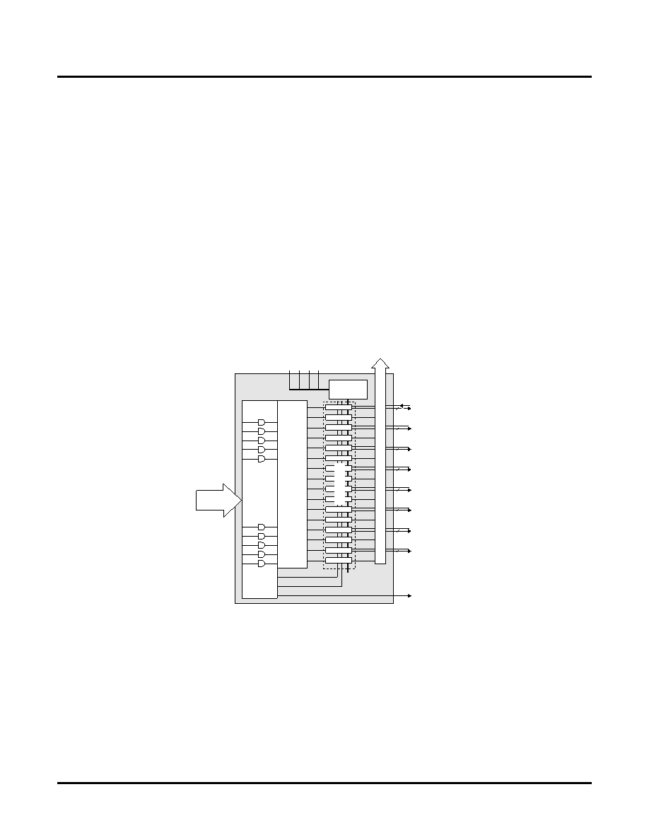
The LA-ispMACH 4000V/Z Automotive GLB consists of a programmable AND array, logic allocator, 16 macrocells
and a GLB clock generator. Macrocells are decoupled from the product terms through the logic allocator and the I/O
pins are decoupled from macrocells through the ORP. Figure 2 illustrates the GLB.
Figure 2. Generic Logic Block
AND Array
The programmable AND Array consists of 36 inputs and 83 output product terms. The 36 inputs from the GRP are
used to form 72 lines in the AND Array (true and complement of the inputs). Each line in the array can be con-
nected to any of the 83 output product terms via a wired-AND. Each of the 80 logic product terms feed the logic
allocator with the remaining three control product terms feeding the Shared PT Clock, Shared PT Initialization and
Shared PT OE. The Shared PT Clock and Shared PT Initialization signals can optionally be inverted before being
fed to the macrocells.
Every set of ve product terms from the 80 logic product terms forms a product term cluster starting with PT0.
There is one product term cluster for every macrocell in the GLB. Figure 3 is a graphical representation of the AND
Array.
Logic
Allocator
36 Inputs
from GRP
16
Macrocells
To
ORP
To GRP
To
Product Term
Output Enable
Sharing
1+OE
16
MC
Feedback
Signals
Clock
Generator
1+OE
CLK0
CLK1
CLK2
CLK3
1+OE
AND
Array
36
Inputs,
83
Product
Terms
相关PDF资料 |
PDF描述 |
|---|---|
| ISPLSI 2096A-100LQN128 | IC PLD ISP 96I/O 10NS 128PQFP |
| ASC08DTES | CONN EDGECARD 16POS .100 EYELET |
| TAP106M016SRS | CAP TANT 10UF 16V 20% RADIAL |
| VE-25D-EV-F3 | CONVERTER MOD DC/DC 85V 150W |
| VE-B5P-CY-F4 | CONVERTER MOD DC/DC 13.8V 50W |
相关代理商/技术参数 |
参数描述 |
|---|---|
| LA4128ZC-75TN128E | 制造商:LATTICE 制造商全称:Lattice Semiconductor 功能描述:3.3V/1.8V In-System Programmable SuperFAST High Density PLDs |
| LA4128ZC-75TN144E | 制造商:LATTICE 制造商全称:Lattice Semiconductor 功能描述:3.3V/1.8V In-System Programmable SuperFAST High Density PLDs |
| LA4128ZC-75TN44E | 制造商:LATTICE 制造商全称:Lattice Semiconductor 功能描述:3.3V/1.8V In-System Programmable SuperFAST High Density PLDs |
| LA4128ZC-75TN48E | 制造商:LATTICE 制造商全称:Lattice Semiconductor 功能描述:3.3V/1.8V In-System Programmable SuperFAST High Density PLDs |
| LA4128ZV-75TN100E | 制造商:LATTICE 制造商全称:Lattice Semiconductor 功能描述:3.3V/1.8V In-System Programmable SuperFAST High Density PLDs |
发布紧急采购,3分钟左右您将得到回复。