- 您现在的位置:买卖IC网 > PDF目录19790 > LAMXO640E-3FTN256E (Lattice Semiconductor Corporation)IC FPGA 640LUTS 256TQFP PDF资料下载
参数资料
| 型号: | LAMXO640E-3FTN256E |
| 厂商: | Lattice Semiconductor Corporation |
| 文件页数: | 4/77页 |
| 文件大小: | 0K |
| 描述: | IC FPGA 640LUTS 256TQFP |
| 标准包装: | 90 |
| 系列: | LA-MachXO |
| 可编程类型: | 系统内可编程 |
| 最大延迟时间 tpd(1): | 4.9ns |
| 电压电源 - 内部: | 1.14 V ~ 1.26 V |
| 宏单元数: | 320 |
| 输入/输出数: | 159 |
| 工作温度: | -40°C ~ 125°C |
| 安装类型: | 表面贴装 |
| 封装/外壳: | 256-LBGA |
| 供应商设备封装: | 256-FTBGA(17x17) |
| 包装: | 托盘 |
第1页第2页第3页当前第4页第5页第6页第7页第8页第9页第10页第11页第12页第13页第14页第15页第16页第17页第18页第19页第20页第21页第22页第23页第24页第25页第26页第27页第28页第29页第30页第31页第32页第33页第34页第35页第36页第37页第38页第39页第40页第41页第42页第43页第44页第45页第46页第47页第48页第49页第50页第51页第52页第53页第54页第55页第56页第57页第58页第59页第60页第61页第62页第63页第64页第65页第66页第67页第68页第69页第70页第71页第72页第73页第74页第75页第76页第77页
2-9
Architecture
Lattice Semiconductor
LA-MachXO Automotive Family Data Sheet
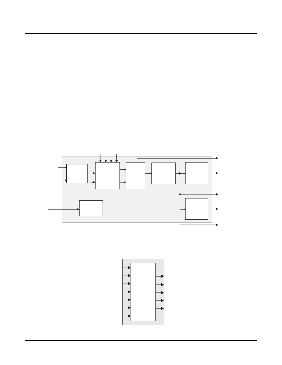
sysCLOCK Phase Locked Loops (PLLs)
The LA-MachXO1200 and LA-MachXO2280 provide PLL support. The source of the PLL input divider can come
from an external pin or from internal routing. There are four sources of feedback signals to the feedback divider:
from CLKINTFB (internal feedback port), from the global clock nets, from the output of the post scalar divider, and
from the routing (or from an external pin). There is a PLL_LOCK signal to indicate that the PLL has locked on to the
input clock signal. Figure 2-10 shows the sysCLOCK PLL diagram.
The setup and hold times of the device can be improved by programming a delay in the feedback or input path of
the PLL which will advance or delay the output clock with reference to the input clock. This delay can be either pro-
grammed during conguration or can be adjusted dynamically. In dynamic mode, the PLL may lose lock after
adjustment and not relock until the tLOCK parameter has been satised. Additionally, the phase and duty cycle block
allows the user to adjust the phase and duty cycle of the CLKOS output.
The sysCLOCK PLLs provide the ability to synthesize clock frequencies. Each PLL has four dividers associated
with it: input clock divider, feedback divider, post scalar divider, and secondary clock divider. The input clock divider
is used to divide the input clock signal, while the feedback divider is used to multiply the input clock signal. The post
scalar divider allows the VCO to operate at higher frequencies than the clock output, thereby increasing the fre-
quency range. The secondary divider is used to derive lower frequency outputs.
Figure 2-10. PLL Diagram
Figure 2-11 shows the available macros for the PLL. Table 2-5 provides signal description of the PLL Block.
Figure 2-11. PLL Primitive
VCO
CLKOS
CLKOK
CLKINTFB
(internal feedback)
LOCK
RST
CLKFB
(from Post Scalar
Divider output,
clock net,
routing/external
pin or CLKINTFB
port
Dynamic Delay Adjustment
Input Clock
Divider
(CLKI)
Feedback
Divider
(CLKFB)
Post Scalar
Divider
(CLKOP)
Phase/Duty
Select
Secondary
Clock
Divider
(CLKOK)
Delay
Adjust
Voltage
Controlled
Oscillator
CLKI
(from routing or
external pin)
CLKOP
EHXPLLC
CLKOS
CLKI
CLKFB
CLKOK
LOCK
RST
CLKOP
DDAIZR
DDAILAG
DDA MODE
DDAIDEL[2:0]
CLKINTFB
相关PDF资料 |
PDF描述 |
|---|---|
| LAMXO640C-3FTN256E | IC FPGA 640LUTS 256TQFP |
| TAP475M016SRW | CAP TANT 4.7UF 16V 20% RADIAL |
| MIC5237-3.3BU | IC REG LDO 3.3V .5A TO263 |
| LCMXO1200E-5M132C | IC PLD 1200LUTS 101I/O 132-BGA |
| MAX5900LAEUT+T | IC HOT-SWAP CONTROLLER SOT23-6 |
相关代理商/技术参数 |
参数描述 |
|---|---|
| LAMXO640E-3TN100E | 功能描述:CPLD - 复杂可编程逻辑器件 Auto Grade (AEC-Q100 ) MachXO640E RoHS:否 制造商:Lattice 系列: 存储类型:EEPROM 大电池数量:128 最大工作频率:333 MHz 延迟时间:2.7 ns 可编程输入/输出端数量:64 工作电源电压:3.3 V 最大工作温度:+ 90 C 最小工作温度:0 C 封装 / 箱体:TQFP-100 |
| LAMXO640E-3TN144E | 功能描述:CPLD - 复杂可编程逻辑器件 Auto Grade (AEC-Q100 ) MachXO640E RoHS:否 制造商:Lattice 系列: 存储类型:EEPROM 大电池数量:128 最大工作频率:333 MHz 延迟时间:2.7 ns 可编程输入/输出端数量:64 工作电源电压:3.3 V 最大工作温度:+ 90 C 最小工作温度:0 C 封装 / 箱体:TQFP-100 |
| LAMXO640LUTSC-3FTN256E | 制造商:LATTICE 制造商全称:Lattice Semiconductor 功能描述:LA-MachXO Automotive Family Data Sheet |
| LAMXO640LUTSC-3FTN324E | 制造商:LATTICE 制造商全称:Lattice Semiconductor 功能描述:LA-MachXO Automotive Family Data Sheet |
| LAMXO640LUTSC-3TN100E | 制造商:LATTICE 制造商全称:Lattice Semiconductor 功能描述:LA-MachXO Automotive Family Data Sheet |
发布紧急采购,3分钟左右您将得到回复。