- 您现在的位置:买卖IC网 > PDF目录177662 > LC4512B-35FN256C (LATTICE SEMICONDUCTOR CORP) PDF资料下载
参数资料
| 型号: | LC4512B-35FN256C |
| 厂商: | LATTICE SEMICONDUCTOR CORP |
| 元件分类: | PLD |
| 中文描述: | EE PLD, 3.5 ns, PBGA256 |
| 封装: | LEAD FREE, FPBGA-256 |
| 文件页数: | 3/99页 |
| 文件大小: | 441K |
| 代理商: | LC4512B-35FN256C |
第1页第2页当前第3页第4页第5页第6页第7页第8页第9页第10页第11页第12页第13页第14页第15页第16页第17页第18页第19页第20页第21页第22页第23页第24页第25页第26页第27页第28页第29页第30页第31页第32页第33页第34页第35页第36页第37页第38页第39页第40页第41页第42页第43页第44页第45页第46页第47页第48页第49页第50页第51页第52页第53页第54页第55页第56页第57页第58页第59页第60页第61页第62页第63页第64页第65页第66页第67页第68页第69页第70页第71页第72页第73页第74页第75页第76页第77页第78页第79页第80页第81页第82页第83页第84页第85页第86页第87页第88页第89页第90页第91页第92页第93页第94页第95页第96页第97页第98页第99页
Lattice Semiconductor
ispMACH 4000V/B/C/Z Family Data Sheet
11
Table 10. ORP Combinations for I/O Blocks with 12 I/Os
ORP Bypass and Fast Output Multiplexers
The ORP bypass and fast-path output multiplexer is a 4:1 multiplexer and allows the 5-PT fast path to bypass the
ORP and be connected directly to the pin with either the regular output or the inverted output. This multiplexer also
allows the register output to bypass the ORP to achieve faster tCO.
Output Enable Routing Multiplexers
The OE Routing Pool provides the corresponding local output enable (OE) product term to the I/O cell.
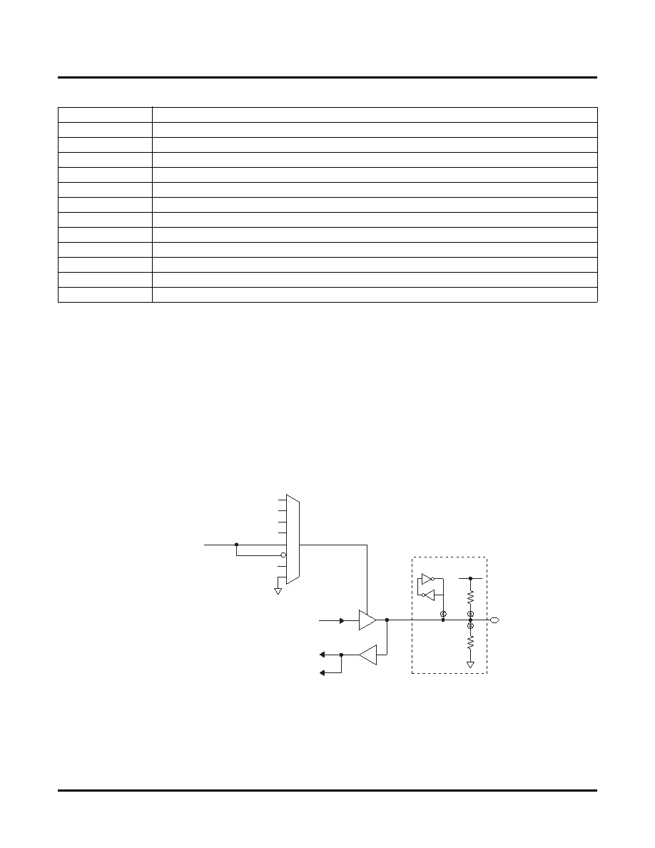
I/O Cell
The I/O cell contains the following programmable elements: output buffer, input buffer, OE multiplexer and bus
maintenance circuitry. Figure 8 details the I/O cell.
Figure 8. I/O Cell
Each output supports a variety of output standards dependent on the VCCO supplied to its I/O bank. Outputs can
also be congured for open drain operation. Each input can be programmed to support a variety of standards, inde-
pendent of the VCCO supplied to its I/O bank. The I/O standards supported are:
I/O Cell
Available Macrocells
I/O 0
M0, M1, M2, M3, M4, M5, M6, M7
I/O 1
M1, M2, M3, M4, M5, M6, M7, M8
I/O 2
M2, M3, M4, M5, M6, M7, M8, M9
I/O 3
M4, M5, M6, M7, M8, M9, M10, M11
I/O 4
M5, M6, M7, M8, M9, M10, M11, M12
I/O 5
M6, M7, M8, M9, M10, M11, M12, M13
I/O 6
M8, M9, M10, M11, M12, M13, M14, M15
I/O 7
M9, M10, M11, M12, M13, M14, M15, M0
I/O 8
M10, M11, M12, M13, M14, M15, M0, M1
I/O 9
M12, M13, M14, M15, M0, M1, M2, M3
I/O 10
M13, M14, M15, M0, M1, M2, M3, M4
I/O 11
M14, M15, M0, M1, M2, M3, M4, M5
GOE 0
From ORP
*Global fuses
From ORP
To Macrocell
To GRP
GOE 1
GOE 2
GOE 3
VCC
VCCO
**
*
相关PDF资料 |
PDF描述 |
|---|---|
| LC4256B-5FN256BC | |
| LC4256C-5FN256BC | |
| LC4256B-10FN256BI | |
| LC4256V-5FN256BC | |
| LC4512B-75FN256C | |
相关代理商/技术参数 |
参数描述 |
|---|---|
| LC4512B-35FN256C1 | 制造商:LATTICE 制造商全称:Lattice Semiconductor 功能描述:3.3V/2.5V/1.8V In-System Programmable SuperFAST High Density PLDs |
| LC4512B-35FT256C | 功能描述:CPLD - 复杂可编程逻辑器件 ispJTAG 2.5V 3.5ns 512MC 208 I/O RoHS:否 制造商:Lattice 系列: 存储类型:EEPROM 大电池数量:128 最大工作频率:333 MHz 延迟时间:2.7 ns 可编程输入/输出端数量:64 工作电源电压:3.3 V 最大工作温度:+ 90 C 最小工作温度:0 C 封装 / 箱体:TQFP-100 |
| LC4512B-35FTN256C | 功能描述:CPLD - 复杂可编程逻辑器件 ispJTAG 2.5V 3.5ns 512MC 208 I/O RoHS:否 制造商:Lattice 系列: 存储类型:EEPROM 大电池数量:128 最大工作频率:333 MHz 延迟时间:2.7 ns 可编程输入/输出端数量:64 工作电源电压:3.3 V 最大工作温度:+ 90 C 最小工作温度:0 C 封装 / 箱体:TQFP-100 |
| LC4512B-35T176C | 功能描述:CPLD - 复杂可编程逻辑器件 PROGRAMMABLE SUPER FAST HI DENSITY PLD RoHS:否 制造商:Lattice 系列: 存储类型:EEPROM 大电池数量:128 最大工作频率:333 MHz 延迟时间:2.7 ns 可编程输入/输出端数量:64 工作电源电压:3.3 V 最大工作温度:+ 90 C 最小工作温度:0 C 封装 / 箱体:TQFP-100 |
| LC4512B-35TN176C | 功能描述:CPLD - 复杂可编程逻辑器件 PROGRAMMABLE SUPER FAST HI DENSITY PLD RoHS:否 制造商:Lattice 系列: 存储类型:EEPROM 大电池数量:128 最大工作频率:333 MHz 延迟时间:2.7 ns 可编程输入/输出端数量:64 工作电源电压:3.3 V 最大工作温度:+ 90 C 最小工作温度:0 C 封装 / 箱体:TQFP-100 |
发布紧急采购,3分钟左右您将得到回复。