- 您现在的位置:买卖IC网 > PDF目录177662 > LC4512B-35FN256C (LATTICE SEMICONDUCTOR CORP) PDF资料下载
参数资料
| 型号: | LC4512B-35FN256C |
| 厂商: | LATTICE SEMICONDUCTOR CORP |
| 元件分类: | PLD |
| 中文描述: | EE PLD, 3.5 ns, PBGA256 |
| 封装: | LEAD FREE, FPBGA-256 |
| 文件页数: | 89/99页 |
| 文件大小: | 441K |
| 代理商: | LC4512B-35FN256C |
第1页第2页第3页第4页第5页第6页第7页第8页第9页第10页第11页第12页第13页第14页第15页第16页第17页第18页第19页第20页第21页第22页第23页第24页第25页第26页第27页第28页第29页第30页第31页第32页第33页第34页第35页第36页第37页第38页第39页第40页第41页第42页第43页第44页第45页第46页第47页第48页第49页第50页第51页第52页第53页第54页第55页第56页第57页第58页第59页第60页第61页第62页第63页第64页第65页第66页第67页第68页第69页第70页第71页第72页第73页第74页第75页第76页第77页第78页第79页第80页第81页第82页第83页第84页第85页第86页第87页第88页当前第89页第90页第91页第92页第93页第94页第95页第96页第97页第98页第99页
Lattice Semiconductor
ispMACH 4000V/B/C/Z Family Data Sheet
9
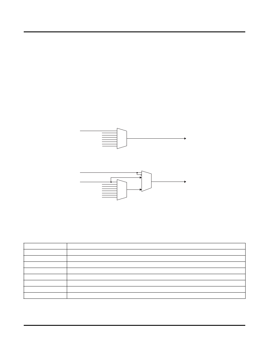
Output Routing Pool (ORP)
The Output Routing Pool allows macrocell outputs to be connected to any of several I/O cells within an I/O block.
This provides greater exibility in determining the pinout and allows design changes to occur without affecting the
pinout. The output routing pool also provides a parallel capability for routing macrocell-level OE product terms. This
allows the OE product term to follow the macrocell output as it is switched between I/O cells. Additionally, the out-
put routing pool allows the macrocell output or true and complement forms of the 5-PT bypass signal to bypass the
output routing multiplexers and feed the I/O cell directly. The enhanced ORP of the ispMACH 4000 family consists
of the following elements:
Output Routing Multiplexers
OE Routing Multiplexers
Output Routing Pool Bypass Multiplexers
Figure 7 shows the structure of the ORP from the I/O cell perspective. This is referred to as an ORP slice. Each
ORP has as many ORP slices as there are I/O cells in the corresponding I/O block.
Figure 7. ORP Slice
Output Routing Multiplexers
The details of connections between the macrocells and the I/O cells vary across devices and within a device
dependent on the maximum number of I/Os available. Tables 5-9 provide the connection details.
Table 6. ORP Combinations for I/O Blocks with 8 I/Os
I/O Cell
Available Macrocells
I/O 0
M0, M1, M2, M3, M4, M5, M6, M7
I/O 1
M2, M3, M4, M5, M6, M7, M8, M9
I/O 2
M4, M5, M6, M7, M8, M9, M10, M11
I/O 3
M6, M7, M8, M9, M10, M11, M12, M13
I/O 4
M8, M9, M10, M11, M12, M13, M14, M15
I/O 5
M10, M11, M12, M13, M14, M15, M0, M1
I/O 6
M12, M13, M14, M15, M0, M1, M2, M3
I/O 7
M14, M15, M0, M1, M2, M3, M4, M5
Output Routing Multiplexer
OE Routing Multiplexer
ORP
Bypass
Multiplexer
From Macrocell
From PTOE
To I/O
Cell
To I/O
Cell
Output
OE
5-PT Fast Path
相关PDF资料 |
PDF描述 |
|---|---|
| LC4256B-5FN256BC | |
| LC4256C-5FN256BC | |
| LC4256B-10FN256BI | |
| LC4256V-5FN256BC | |
| LC4512B-75FN256C | |
相关代理商/技术参数 |
参数描述 |
|---|---|
| LC4512B-35FN256C1 | 制造商:LATTICE 制造商全称:Lattice Semiconductor 功能描述:3.3V/2.5V/1.8V In-System Programmable SuperFAST High Density PLDs |
| LC4512B-35FT256C | 功能描述:CPLD - 复杂可编程逻辑器件 ispJTAG 2.5V 3.5ns 512MC 208 I/O RoHS:否 制造商:Lattice 系列: 存储类型:EEPROM 大电池数量:128 最大工作频率:333 MHz 延迟时间:2.7 ns 可编程输入/输出端数量:64 工作电源电压:3.3 V 最大工作温度:+ 90 C 最小工作温度:0 C 封装 / 箱体:TQFP-100 |
| LC4512B-35FTN256C | 功能描述:CPLD - 复杂可编程逻辑器件 ispJTAG 2.5V 3.5ns 512MC 208 I/O RoHS:否 制造商:Lattice 系列: 存储类型:EEPROM 大电池数量:128 最大工作频率:333 MHz 延迟时间:2.7 ns 可编程输入/输出端数量:64 工作电源电压:3.3 V 最大工作温度:+ 90 C 最小工作温度:0 C 封装 / 箱体:TQFP-100 |
| LC4512B-35T176C | 功能描述:CPLD - 复杂可编程逻辑器件 PROGRAMMABLE SUPER FAST HI DENSITY PLD RoHS:否 制造商:Lattice 系列: 存储类型:EEPROM 大电池数量:128 最大工作频率:333 MHz 延迟时间:2.7 ns 可编程输入/输出端数量:64 工作电源电压:3.3 V 最大工作温度:+ 90 C 最小工作温度:0 C 封装 / 箱体:TQFP-100 |
| LC4512B-35TN176C | 功能描述:CPLD - 复杂可编程逻辑器件 PROGRAMMABLE SUPER FAST HI DENSITY PLD RoHS:否 制造商:Lattice 系列: 存储类型:EEPROM 大电池数量:128 最大工作频率:333 MHz 延迟时间:2.7 ns 可编程输入/输出端数量:64 工作电源电压:3.3 V 最大工作温度:+ 90 C 最小工作温度:0 C 封装 / 箱体:TQFP-100 |
发布紧急采购,3分钟左右您将得到回复。