- 您现在的位置:买卖IC网 > PDF目录19631 > LC51024MV-52F672C (Lattice Semiconductor Corporation)IC XPLD 1024MC 5.2NS 672FPBGA PDF资料下载
参数资料
| 型号: | LC51024MV-52F672C |
| 厂商: | Lattice Semiconductor Corporation |
| 文件页数: | 6/99页 |
| 文件大小: | 0K |
| 描述: | IC XPLD 1024MC 5.2NS 672FPBGA |
| 标准包装: | 40 |
| 系列: | ispXPLD® 5000MV |
| 可编程类型: | 系统内可编程 |
| 最大延迟时间 tpd(1): | 5.2ns |
| 电压电源 - 内部: | 3 V ~ 3.6 V |
| 逻辑元件/逻辑块数目: | 32 |
| 宏单元数: | 1024 |
| 输入/输出数: | 381 |
| 工作温度: | 0°C ~ 90°C |
| 安装类型: | 表面贴装 |
| 封装/外壳: | 672-BBGA |
| 供应商设备封装: | 672-FPBGA(27x27) |
| 包装: | 托盘 |
第1页第2页第3页第4页第5页当前第6页第7页第8页第9页第10页第11页第12页第13页第14页第15页第16页第17页第18页第19页第20页第21页第22页第23页第24页第25页第26页第27页第28页第29页第30页第31页第32页第33页第34页第35页第36页第37页第38页第39页第40页第41页第42页第43页第44页第45页第46页第47页第48页第49页第50页第51页第52页第53页第54页第55页第56页第57页第58页第59页第60页第61页第62页第63页第64页第65页第66页第67页第68页第69页第70页第71页第72页第73页第74页第75页第76页第77页第78页第79页第80页第81页第82页第83页第84页第85页第86页第87页第88页第89页第90页第91页第92页第93页第94页第95页第96页第97页第98页第99页
Lattice Semiconductor
ispXPLD 5000MX Family Data Sheet
10
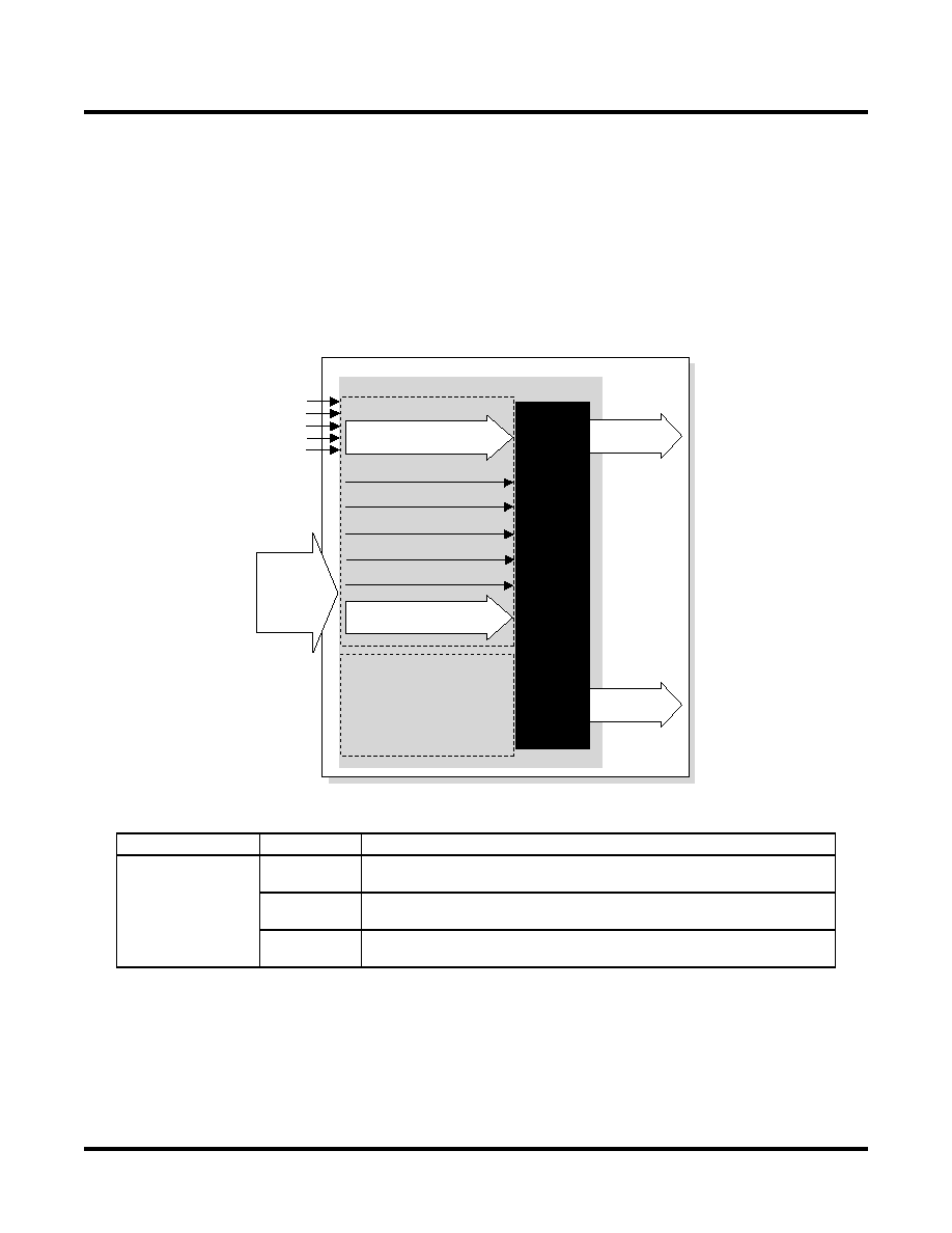
True Dual-Port SRAM Mode
In Dual-Port SRAM Mode the multi-function array is configured as a dual port SRAM. In this mode two independent
read/write ports access the same 8,192-bits of memory. Data widths of 1, 2, 4, 8, and 16 are supported by the
MFB. Figure 9 shows the block diagram of the dual port SRAM.
Write data, address, chip select and read/write signals are always synchronous (registered.) The output data sig-
nals can be synchronous or asynchronous. Resets are asynchronous. All inputs on the same port share the same
clock, clock enable, and reset selections. All outputs on the same port share the same clock, clock enable, and
reset selections. Selections may be made independently between both inputs and outputs and ports. Table 5
shows the possible sources for the clock, clock enable and initialization signals for the various registers.
Figure 9. Dual-Port SRAM Block Diagram
Table 5. Register Clock, Clock Enable, and Reset in Dual-Port SRAM Mode
Register
Input
Source
Address, Write Data,
Read Data, Read/
Write, and Chip
Select
Clock
CLKA (CLKB) or one of the global clocks (CLK0 - CLK3). The selected sig-
nal can be inverted if desired.
Clock Enable
CENA (CENB) or one of the global clocks (CLK1 - CLK 2). The selected sig-
nal can be inverted if required.
Reset
Created by the logical OR of the global reset signal and RSTA (RSTB).
RSTA (RSTB) can be inverted is desired.
‘
Read/Write Address
(ADA[0:8-12])
Clock A (CLKA)
Write/Read A (WRA)
Reset A (RSTA)
68 Inputs
From
Routing
Dual
Port
SRAM
Array
PORT A
PORT B
Similar signals
as PORT A:
ADB[0:8-12], RSTB,
CLKB, CENB, WRB,
CSB[0,1], DIB[0:0,1,3,7,15]
Write Data
(DIA[0:0,1,3,7,15])
Chip Sel A (CSA [0:1])
Clk En A (CENA)
RESET
CLK0
CLK3
CLK1
CLK2
RD Data A
(DOA[0:0-15])
RD Data B
(DOB[0:0-15])
SELECT
DEVICES
DISCONTINUED
相关PDF资料 |
PDF描述 |
|---|---|
| VE-BTZ-CX-F3 | CONVERTER MOD DC/DC 2V 30W |
| VE-BWK-CX-B1 | CONVERTER MOD DC/DC 40V 75W |
| ZWS240PAF24 | PWR SUP 24V 240W 10A |
| 180-062-113R001 | CONN DB62 MALE HD DIP SLD NICKEL |
| VE-BWK-CW-B1 | CONVERTER MOD DC/DC 40V 100W |
相关代理商/技术参数 |
参数描述 |
|---|---|
| LC51024MV-52F672I | 制造商:LATTICE 制造商全称:Lattice Semiconductor 功能描述:3.3V, 2.5V and 1.8V In-System Programmable eXpanded Programmable Logic Device XPLD⑩ Family |
| LC51024MV-52FN208C | 制造商:LATTICE 制造商全称:Lattice Semiconductor 功能描述:3.3V, 2.5V and 1.8V In-System Programmable eXpanded Programmable Logic Device XPLD⑩ Family |
| LC51024MV-52FN208I | 制造商:LATTICE 制造商全称:Lattice Semiconductor 功能描述:3.3V, 2.5V and 1.8V In-System Programmable eXpanded Programmable Logic Device XPLD⑩ Family |
| LC51024MV-52FN256C | 制造商:LATTICE 制造商全称:Lattice Semiconductor 功能描述:3.3V, 2.5V and 1.8V In-System Programmable eXpanded Programmable Logic Device XPLD⑩ Family |
| LC51024MV-52FN256I | 制造商:LATTICE 制造商全称:Lattice Semiconductor 功能描述:3.3V, 2.5V and 1.8V In-System Programmable eXpanded Programmable Logic Device XPLD⑩ Family |
发布紧急采购,3分钟左右您将得到回复。