- 您现在的位置:买卖IC网 > PDF目录177663 > LC5256B-10T128I (LATTICE SEMICONDUCTOR CORP) PDF资料下载
参数资料
| 型号: | LC5256B-10T128I |
| 厂商: | LATTICE SEMICONDUCTOR CORP |
| 元件分类: | PLD |
| 中文描述: | EE PLD, 12 ns, PQFP128 |
| 封装: | TQFP-128 |
| 文件页数: | 45/66页 |
| 文件大小: | 240K |
| 代理商: | LC5256B-10T128I |
第1页第2页第3页第4页第5页第6页第7页第8页第9页第10页第11页第12页第13页第14页第15页第16页第17页第18页第19页第20页第21页第22页第23页第24页第25页第26页第27页第28页第29页第30页第31页第32页第33页第34页第35页第36页第37页第38页第39页第40页第41页第42页第43页第44页当前第45页第46页第47页第48页第49页第50页第51页第52页第53页第54页第55页第56页第57页第58页第59页第60页第61页第62页第63页第64页第65页第66页
Lattice Semiconductor
ispMACH 5000B Family Data Sheet
5
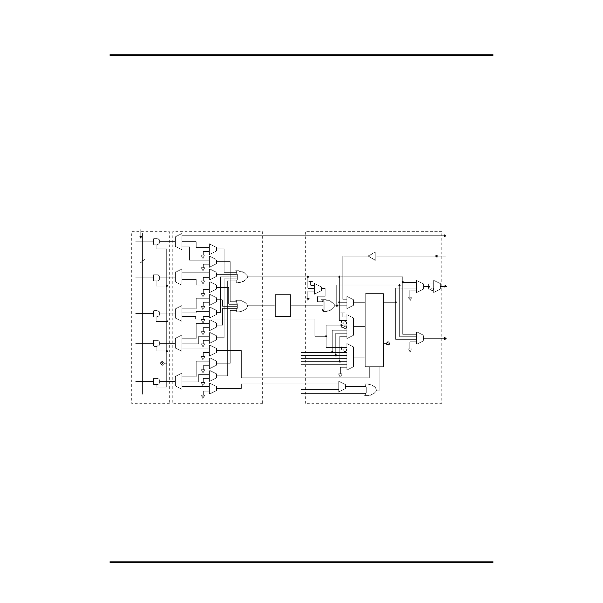
Macrocell
The 32 registered macrocells in the GLB are driven by the 32 outputs from the PTSA or the PTSA bypass. Each
macrocell contains a programmable XOR gate, a programmable register/latch ip-op and the necessary clocks
and control logic to allow combinatorial or registered operation.
The macrocells each have two outputs, which can be fed to the GRP and I/O cell. This dual or concurrent output
capability from the macrocell gives efcient use of the hardware resources. One output can be a registered function
for example, while the other output can be an unrelated combinatorial function. A direct register input from the I/O
cell facilitates efcient use of the macrocell to construct high-speed input registers.
Macrocell registers can be clocked from one of several global or product term clocks available on the device. A glo-
bal and product term clock enable is also provided, eliminating the need to gate the clock to the macrocell registers
directly. Reset and preset for the macrocell register is provided from both global and product term signals. The
macrocell register can be programmed to operate as a D-type register or a D-type latch. Figure 5 is a graphical rep-
resentation of the ispMACH 5000B macrocell.
Figure 5. ispMACH 5000B Macrocell
I/O Cell
The ispMACH 5000B I/O cell provides a high degree of exibility. It includes the sysIO feature and an enhanced
output enable MUX for optimal performance both on- and off-chip. The sysIO feature allows I/O cells to be cong-
ured to different I/O standards, drive strengths and slew rates. The enhanced output enable MUX provides up to 14
different output enable choices per I/O cell.
The I/O cell contains an output enable (OE) MUX, a programmable tri-state output buffer, a programmable input
buffer, a programmable pull-up resistor, a programmable pull-down resistor and a programmable bus-friendly latch.
The I/O cell receives its input from its associated macrocell. The I/O cell has a feedback line to its associated mac-
rocell and a direct path to the GRP.
The output enable (OE) MUX selects the OE signal per I/O cell. The inputs to the OE MUX are the four shared
PTOE signals, PTOE, the two GOE signals. The OE MUX also has the ability to choose either the true or inverse of
From
GRP
68
Speed/
Power
PTSA
PTSA Bypass
PT OE to
I/O Block
From
I/O Cell
PT Clock
PT Preset
PT Reset
Shared PT Reset
Shared PT Clock
CLK0
CLK1
CLK2
CLK3
Global Reset
Clk En
Clk
R/L
D
PR
Q
AND Array
Dual-OR Array
Macrocell
Output
to I/O Block
GRP
Discontinued
Product
(PCN
#02-06).
Contact
Rochester
Electronics
for
Availability.
www.latticesemi.com/sales/discontinueddevicessales.cfm
相关PDF资料 |
PDF描述 |
|---|---|
| LC5256B-75Q208I | |
| LC5256B-5Q208C | |
| LC5384B-4F256C | |
| LC5256B-4Q208C | |
| LC5384B-5Q208C | |
相关代理商/技术参数 |
参数描述 |
|---|---|
| LC5256B-4F256C | 功能描述:CPLD - 复杂可编程逻辑器件 PROGRAM EXPANDED LOG RoHS:否 制造商:Lattice 系列: 存储类型:EEPROM 大电池数量:128 最大工作频率:333 MHz 延迟时间:2.7 ns 可编程输入/输出端数量:64 工作电源电压:3.3 V 最大工作温度:+ 90 C 最小工作温度:0 C 封装 / 箱体:TQFP-100 |
| LC5256B-4Q208C | 功能描述:CPLD - 复杂可编程逻辑器件 PROGRAM EXPANDED LOG RoHS:否 制造商:Lattice 系列: 存储类型:EEPROM 大电池数量:128 最大工作频率:333 MHz 延迟时间:2.7 ns 可编程输入/输出端数量:64 工作电源电压:3.3 V 最大工作温度:+ 90 C 最小工作温度:0 C 封装 / 箱体:TQFP-100 |
| LC5256B-4T128C | 功能描述:CPLD - 复杂可编程逻辑器件 PROGRAM EXPANDED LOG RoHS:否 制造商:Lattice 系列: 存储类型:EEPROM 大电池数量:128 最大工作频率:333 MHz 延迟时间:2.7 ns 可编程输入/输出端数量:64 工作电源电压:3.3 V 最大工作温度:+ 90 C 最小工作温度:0 C 封装 / 箱体:TQFP-100 |
| LC5256B-5F256C | 功能描述:CPLD - 复杂可编程逻辑器件 PROGRAM EXPANDED LOG RoHS:否 制造商:Lattice 系列: 存储类型:EEPROM 大电池数量:128 最大工作频率:333 MHz 延迟时间:2.7 ns 可编程输入/输出端数量:64 工作电源电压:3.3 V 最大工作温度:+ 90 C 最小工作温度:0 C 封装 / 箱体:TQFP-100 |
| LC5256B-5F256I | 功能描述:CPLD - 复杂可编程逻辑器件 PROGRAM EXPANDED LOG RoHS:否 制造商:Lattice 系列: 存储类型:EEPROM 大电池数量:128 最大工作频率:333 MHz 延迟时间:2.7 ns 可编程输入/输出端数量:64 工作电源电压:3.3 V 最大工作温度:+ 90 C 最小工作温度:0 C 封装 / 箱体:TQFP-100 |
发布紧急采购,3分钟左右您将得到回复。