- 您现在的位置:买卖IC网 > PDF目录67755 > LC5511D POWER FACTOR CONTROLLER, 18 kHz SWITCHING FREQ-MAX, DIP7 PDF资料下载
参数资料
| 型号: | LC5511D |
| 元件分类: | 稳压器 |
| 英文描述: | POWER FACTOR CONTROLLER, 18 kHz SWITCHING FREQ-MAX, DIP7 |
| 封装: | DIP-8/7 |
| 文件页数: | 28/40页 |
| 文件大小: | 888K |
| 代理商: | LC5511D |
第1页第2页第3页第4页第5页第6页第7页第8页第9页第10页第11页第12页第13页第14页第15页第16页第17页第18页第19页第20页第21页第22页第23页第24页第25页第26页第27页当前第28页第29页第30页第31页第32页第33页第34页第35页第36页第37页第38页第39页第40页
34
Allegro MicroSystems, Inc.
115 Northeast Cutoff
Worcester, Massachusetts 01615-0036 U.S.A.
1.508.853.5000; www.allegromicro.com
28106.02
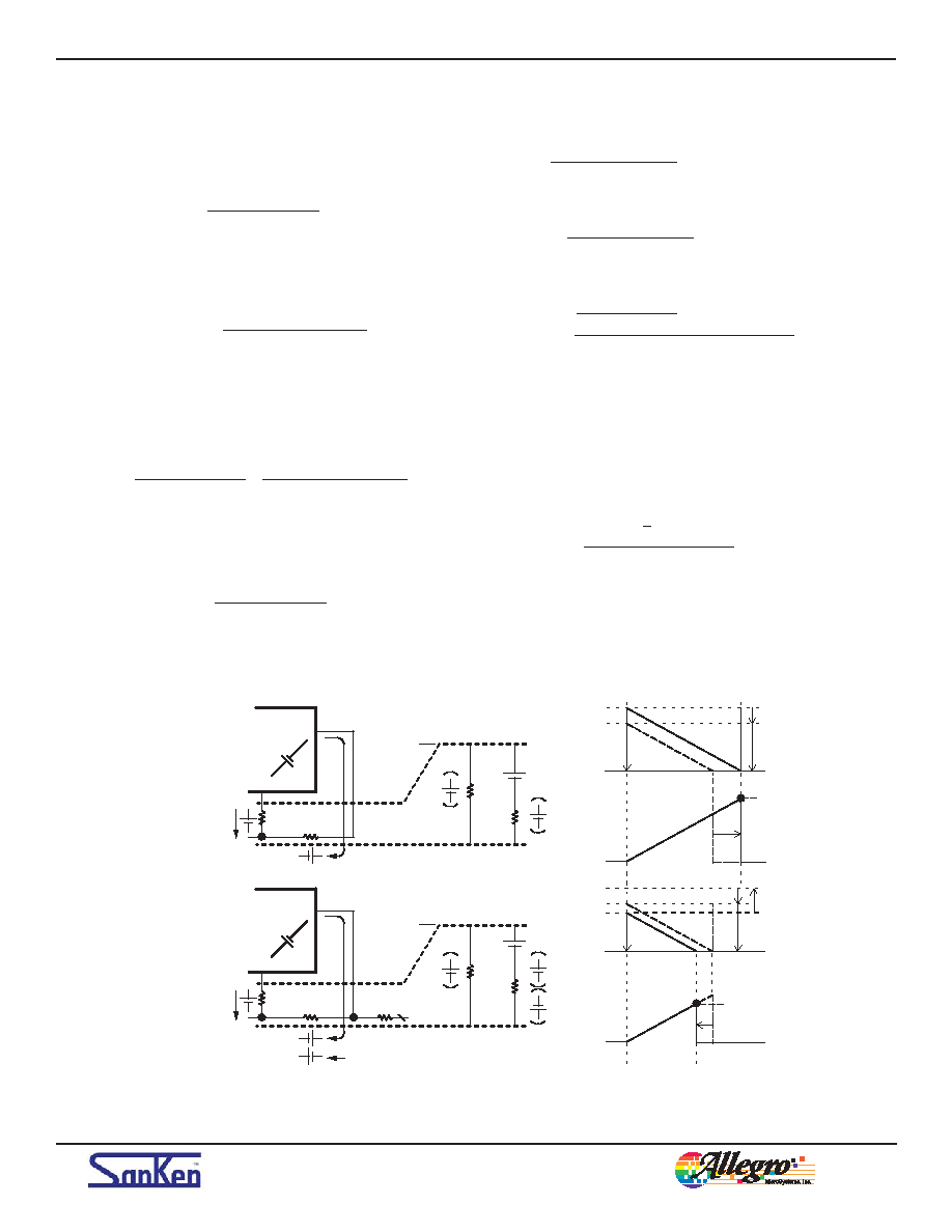
1. The overcurrent detecting drain peak current, IDP, without
the input compensation circuit, is expressed by the following,
based on equation 6, from figure 49, upper panel:
=
IDP
ROCP
VOCP + R3 × IOCP
(8)
2. On the other hand, the overcurrent detecting drain peak cur-
rent, I'DP, with the input compensation circuit, is expressed
by the following, based on equation 7, from figure. 49, lower
panel:
=
I 'DP
ROCP
VOCP + R3 × (IOCP – I )
(9)
Here, I'DP is the drain peak current where the output power
of the maximum AC input voltage becomes the same as that
limited by OCP at the minimum AC input voltage.
3. From equations 8 and 9, the compensation current, I, of the
input compensation circuit, is expressed as follows:
=
I DP – I 'DP
( I
DP – I 'DP )
I
–
ROCP
VOCP + R3 × (IOCP – I )
ROCP
VOCP + R3 × IOCP
=
× R
OCP / R
3
(10)
4. The forward voltage, Efw1 , at C2 peak voltage EIN(PK)(max) is
expressed as follows:
N
P
N
D × EIN(PK)(max)
=
E
fw1
(11)
5. Next, RX1 is expressed by the following, in order to let the
compensation current, I, flow at the maximum AC input volt-
age, EIN(PK)(max):
Efw1 – DZX1 – VFX1
RX1 + R3 + ROCP
=
I
(12)
assuming: R3, ROCP << RX1
I
Efw1 – DZX1 – VFX1
=
RX1
(13)
from equations 11 and 13:
–
I
(DZX1 + VFX1 )
=
NP
RX1
ND × EIN(PK)(max)
(14)
AC input compensation circuit design example with universal
input
Tentatively target the center point voltage between the minimum
AC input voltage and the middle of the universal input, where
the input compensation starts.
Decide IDP and I 'DP at both minimum and maximum AC input
voltage, when the output is set to the target value for both con-
ditions. For this, use the formula:
=
I'DP
D'ON× η1 × η2×VAC(min)
2√2× PO
(15)
In the case of using equation 15, enter minimum and maximum
AC input voltages as the parameter of VAC(min) and D'ON at
those voltages as the parameter of D'ON. Alternatively, measure
those drain currents using an actual power supply board.
Figure 49. Compensated drain current waveforms
R3
×
ROCP×IDP
R3 ×
IDP
Increase
Decrease
ROCP
IOCP
I
IOCP
× I
× IOCP
IDP
ID
IDP
×
R3 ×
ROCP×
R3
VOCP
R3
ROCP ×IDP
'
IDP
'
IDP
'
IDP
'
S/GND
OCP
ROCP
R3
RX1
ROCP
R3
S/GND
OCP
1(2)
With input
compensation
circuit
Without input
compensation
circuit
VOCP
3(5)
VOCP
IOCP
I
S/GND
相关PDF资料 |
PDF描述 |
|---|---|
| LC5521D | 2.5 A POWER FACTOR CONTROLLER, 18 kHz SWITCHING FREQ-MAX, DIP7 |
| LC72137 | PLL FREQUENCY SYNTHESIZER, 40 MHz, PDIP22 |
| LC72137M | PLL FREQUENCY SYNTHESIZER, 40 MHz, PDSO20 |
| LC72137 | PLL FREQUENCY SYNTHESIZER, 40 MHz, PDIP22 |
| LC72137M | PLL FREQUENCY SYNTHESIZER, 40 MHz, PDSO20 |
相关代理商/技术参数 |
参数描述 |
|---|---|
| LC5512B-10F256C | 功能描述:CPLD - 复杂可编程逻辑器件 PROGRAM EXPANDED LOG RoHS:否 制造商:Lattice 系列: 存储类型:EEPROM 大电池数量:128 最大工作频率:333 MHz 延迟时间:2.7 ns 可编程输入/输出端数量:64 工作电源电压:3.3 V 最大工作温度:+ 90 C 最小工作温度:0 C 封装 / 箱体:TQFP-100 |
| LC5512B-10F256I | 功能描述:CPLD - 复杂可编程逻辑器件 PROGRAM EXPANDED LOG RoHS:否 制造商:Lattice 系列: 存储类型:EEPROM 大电池数量:128 最大工作频率:333 MHz 延迟时间:2.7 ns 可编程输入/输出端数量:64 工作电源电压:3.3 V 最大工作温度:+ 90 C 最小工作温度:0 C 封装 / 箱体:TQFP-100 |
| LC5512B-10F484C | 功能描述:CPLD - 复杂可编程逻辑器件 Use ispMACH 4000B RoHS:否 制造商:Lattice 系列: 存储类型:EEPROM 大电池数量:128 最大工作频率:333 MHz 延迟时间:2.7 ns 可编程输入/输出端数量:64 工作电源电压:3.3 V 最大工作温度:+ 90 C 最小工作温度:0 C 封装 / 箱体:TQFP-100 |
| LC5512B-10F484I | 功能描述:CPLD - 复杂可编程逻辑器件 Use ispMACH 4000B RoHS:否 制造商:Lattice 系列: 存储类型:EEPROM 大电池数量:128 最大工作频率:333 MHz 延迟时间:2.7 ns 可编程输入/输出端数量:64 工作电源电压:3.3 V 最大工作温度:+ 90 C 最小工作温度:0 C 封装 / 箱体:TQFP-100 |
| LC5512B-10Q208C | 功能描述:CPLD - 复杂可编程逻辑器件 Use ispMACH 4000B RoHS:否 制造商:Lattice 系列: 存储类型:EEPROM 大电池数量:128 最大工作频率:333 MHz 延迟时间:2.7 ns 可编程输入/输出端数量:64 工作电源电压:3.3 V 最大工作温度:+ 90 C 最小工作温度:0 C 封装 / 箱体:TQFP-100 |
发布紧急采购,3分钟左右您将得到回复。