- 您现在的位置:买卖IC网 > PDF目录67755 > LC5511D POWER FACTOR CONTROLLER, 18 kHz SWITCHING FREQ-MAX, DIP7 PDF资料下载
参数资料
| 型号: | LC5511D |
| 元件分类: | 稳压器 |
| 英文描述: | POWER FACTOR CONTROLLER, 18 kHz SWITCHING FREQ-MAX, DIP7 |
| 封装: | DIP-8/7 |
| 文件页数: | 31/40页 |
| 文件大小: | 888K |
| 代理商: | LC5511D |
第1页第2页第3页第4页第5页第6页第7页第8页第9页第10页第11页第12页第13页第14页第15页第16页第17页第18页第19页第20页第21页第22页第23页第24页第25页第26页第27页第28页第29页第30页当前第31页第32页第33页第34页第35页第36页第37页第38页第39页第40页
37
Allegro MicroSystems, Inc.
115 Northeast Cutoff
Worcester, Massachusetts 01615-0036 U.S.A.
1.508.853.5000; www.allegromicro.com
28106.02
susceptible to radiation noise; therefore, widen and shorten it.
Consider the local safety regulations for component layouts
and trace designs where high frequency and voltage appear. In
addition, note that the power MOSFET on-resistance RDS(on) has
a positive characteristic relative to temperature, and therefore,
consider it for thermal design.
Figures 53, 54, and 55 show practical trace design examples and
considerations for the LC551xD, LC552xD and LC552xF series
respectively. In addition, observe the following:
Traces among the S/GND pin, ROCP, C2, T1(primary winding),
and D/ST pin:
The traces carry the switching current; therefore, widen and
shorten them as much as possible.
If the IC and the electrolytic capacitor C2 are apart, place a film
capacitor (0.1 μF with appropriate voltage rating) close to the
IC or the transformer in order to reduce series inductances of
the traces against high frequency current.
Traces among the S/GND pin, C4(–), T1(auxiliary winding D),
R1, D5, C4(+), and VCC pin:
This trace is for supplying voltage to IC. Widen and shorten the
traces as much as possible. If the IC and the electrolytic capaci-
tor C4 are apart, place a film or ceramic capacitor (0.1 to 1.0 μF
/ 50 V) as close to VCC pin and the S/GND pin as possible.
Current Sensing Resistor ROCP:
Place ROCP as close to the S/GND pin as possible. In addi-
tion, in order to avoid interference of the switching current to
the control circuit, connect the ground of the control circuit to
S/GND as close as possible.
Connect R3 as close to ROCP as possible (at point A of figures
53, 54, and 55) with dedicated traces.
Secondary side, traces among T1(secondary winding S), D8,
and C10:
The secondary-side switching current runs through this trace.
Widen and shorten the traces as much as possible.
Thin and long traces cause the series inductance to be high and
it results in high surge voltage on the power MOSFET when
it turns off. Therefore, proper layout pattern design helps to
increase voltage margin of the power MOSFET to its break-
down voltage and reduce power stress and loss of the clamping
snubber circuit.
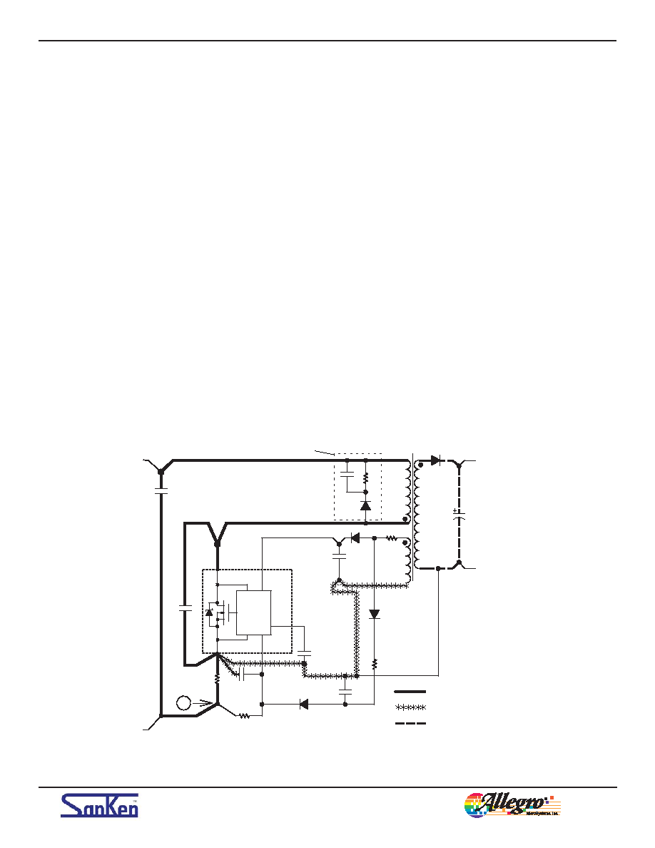
Figure 53. LC551xD (non-isolated designs) peripheral circuit connection example
Main circuit
Control circuit GND circuit
Secondary rectification circuit
Z1
Con-
troller
Chip
S
D
P
C4
S/GND
OCP
3
1
2
8
D6
ROCP
A
C5
D8
C10
T1
D5
C3
C2
D7
COMP
C6
VCC
D/ST
R1
R3
R4
C7
4
Clamping snubber
LC551xD
相关PDF资料 |
PDF描述 |
|---|---|
| LC5521D | 2.5 A POWER FACTOR CONTROLLER, 18 kHz SWITCHING FREQ-MAX, DIP7 |
| LC72137 | PLL FREQUENCY SYNTHESIZER, 40 MHz, PDIP22 |
| LC72137M | PLL FREQUENCY SYNTHESIZER, 40 MHz, PDSO20 |
| LC72137 | PLL FREQUENCY SYNTHESIZER, 40 MHz, PDIP22 |
| LC72137M | PLL FREQUENCY SYNTHESIZER, 40 MHz, PDSO20 |
相关代理商/技术参数 |
参数描述 |
|---|---|
| LC5512B-10F256C | 功能描述:CPLD - 复杂可编程逻辑器件 PROGRAM EXPANDED LOG RoHS:否 制造商:Lattice 系列: 存储类型:EEPROM 大电池数量:128 最大工作频率:333 MHz 延迟时间:2.7 ns 可编程输入/输出端数量:64 工作电源电压:3.3 V 最大工作温度:+ 90 C 最小工作温度:0 C 封装 / 箱体:TQFP-100 |
| LC5512B-10F256I | 功能描述:CPLD - 复杂可编程逻辑器件 PROGRAM EXPANDED LOG RoHS:否 制造商:Lattice 系列: 存储类型:EEPROM 大电池数量:128 最大工作频率:333 MHz 延迟时间:2.7 ns 可编程输入/输出端数量:64 工作电源电压:3.3 V 最大工作温度:+ 90 C 最小工作温度:0 C 封装 / 箱体:TQFP-100 |
| LC5512B-10F484C | 功能描述:CPLD - 复杂可编程逻辑器件 Use ispMACH 4000B RoHS:否 制造商:Lattice 系列: 存储类型:EEPROM 大电池数量:128 最大工作频率:333 MHz 延迟时间:2.7 ns 可编程输入/输出端数量:64 工作电源电压:3.3 V 最大工作温度:+ 90 C 最小工作温度:0 C 封装 / 箱体:TQFP-100 |
| LC5512B-10F484I | 功能描述:CPLD - 复杂可编程逻辑器件 Use ispMACH 4000B RoHS:否 制造商:Lattice 系列: 存储类型:EEPROM 大电池数量:128 最大工作频率:333 MHz 延迟时间:2.7 ns 可编程输入/输出端数量:64 工作电源电压:3.3 V 最大工作温度:+ 90 C 最小工作温度:0 C 封装 / 箱体:TQFP-100 |
| LC5512B-10Q208C | 功能描述:CPLD - 复杂可编程逻辑器件 Use ispMACH 4000B RoHS:否 制造商:Lattice 系列: 存储类型:EEPROM 大电池数量:128 最大工作频率:333 MHz 延迟时间:2.7 ns 可编程输入/输出端数量:64 工作电源电压:3.3 V 最大工作温度:+ 90 C 最小工作温度:0 C 封装 / 箱体:TQFP-100 |
发布紧急采购,3分钟左右您将得到回复。