- 您现在的位置:买卖IC网 > PDF目录67755 > LC5511D POWER FACTOR CONTROLLER, 18 kHz SWITCHING FREQ-MAX, DIP7 PDF资料下载
参数资料
| 型号: | LC5511D |
| 元件分类: | 稳压器 |
| 英文描述: | POWER FACTOR CONTROLLER, 18 kHz SWITCHING FREQ-MAX, DIP7 |
| 封装: | DIP-8/7 |
| 文件页数: | 9/40页 |
| 文件大小: | 888K |
| 代理商: | LC5511D |
第1页第2页第3页第4页第5页第6页第7页第8页当前第9页第10页第11页第12页第13页第14页第15页第16页第17页第18页第19页第20页第21页第22页第23页第24页第25页第26页第27页第28页第29页第30页第31页第32页第33页第34页第35页第36页第37页第38页第39页第40页
17
Allegro MicroSystems, Inc.
115 Northeast Cutoff
Worcester, Massachusetts 01615-0036 U.S.A.
1.508.853.5000; www.allegromicro.com
28106.02
Operation Description
All of the parameter values used in these descriptions are typi-
cal values, unless they are specified as minimum or maximum.
This section describes IC operations as it is used for LED lighting
power supply applications. About current direction, "+" indicates
sink flow toward the IC and "–" indicates source flow from the
IC. The pin numbers parenthesized represent LC552xF numbers.
On-Width Control Operation
LC551xD series (non-isolated designs)
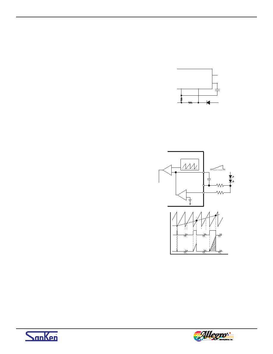
Figure 12 shows the
peripheral circuit at the COMP pin of the LC551xD, and figure 13
shows the on-width control. The output control is done by voltage
mode control, which controls on-width depending on output load
and average current control.
As showed in figure 13, in the average current control operation,
the output current sensing resistor voltage is compared against the
reference voltage by the OTA circuit, and its output is averaged at
COMP pin. This voltage is compared against the internal oscilla-
tor (OSC) by the FB comparator in order to control the on-width
for the average current control operation. Here, OSC indicates
the oscillator circuit, which controls the minimum oscillating
frequency, quasi-resonant oscillation, and the maximum on-time
limit.
The constant output current control of the output is done as
below:
If the output load current becomes less than the target value, the
ISENSE pin voltage will become low. This causes the averaged
OTA circuit output voltage at the COMP pin to become high,
which increases the on-width and the output current.
If the output current becomes greater than the target value, the
circuits operate in the opposite way. The averaged voltage at
the COMP pin will become low, and resulting reductions in the
on-width and the output current.
Figure 14 shows the average input current waveform. The aver-
aged COMP pin voltage becomes constant, and the duty cycle
control becomes based on the EIN voltage (C2 voltage in figure 9).
It makes an averaged input current sine waveform which realizes
a high power factor.
LC552xD and LC552xF series (isolated designs)
Figure 15
shows the peripheral circuit at the FB pin of the LC551xD/
LC552xF, and figure 16 shows the on-width control. The output
Figure 13. On-width control, LC551xD series
1
–
+
–
+
4
6
FB
OTA
LED
Current
LC551xD
sensing
resistor
ISENSE
S/GND
COMP
COMP pin
voltage
Gate
on-width
Gate on-width
Drain current
OSC
V
COMP
OSC
3
1
COMP
R OCP
C6
S/GND
ISENSE
D7
OCP
LC551xD
R3
6
4
Figure 12. COMP pin peripheral circuit
相关PDF资料 |
PDF描述 |
|---|---|
| LC5521D | 2.5 A POWER FACTOR CONTROLLER, 18 kHz SWITCHING FREQ-MAX, DIP7 |
| LC72137 | PLL FREQUENCY SYNTHESIZER, 40 MHz, PDIP22 |
| LC72137M | PLL FREQUENCY SYNTHESIZER, 40 MHz, PDSO20 |
| LC72137 | PLL FREQUENCY SYNTHESIZER, 40 MHz, PDIP22 |
| LC72137M | PLL FREQUENCY SYNTHESIZER, 40 MHz, PDSO20 |
相关代理商/技术参数 |
参数描述 |
|---|---|
| LC5512B-10F256C | 功能描述:CPLD - 复杂可编程逻辑器件 PROGRAM EXPANDED LOG RoHS:否 制造商:Lattice 系列: 存储类型:EEPROM 大电池数量:128 最大工作频率:333 MHz 延迟时间:2.7 ns 可编程输入/输出端数量:64 工作电源电压:3.3 V 最大工作温度:+ 90 C 最小工作温度:0 C 封装 / 箱体:TQFP-100 |
| LC5512B-10F256I | 功能描述:CPLD - 复杂可编程逻辑器件 PROGRAM EXPANDED LOG RoHS:否 制造商:Lattice 系列: 存储类型:EEPROM 大电池数量:128 最大工作频率:333 MHz 延迟时间:2.7 ns 可编程输入/输出端数量:64 工作电源电压:3.3 V 最大工作温度:+ 90 C 最小工作温度:0 C 封装 / 箱体:TQFP-100 |
| LC5512B-10F484C | 功能描述:CPLD - 复杂可编程逻辑器件 Use ispMACH 4000B RoHS:否 制造商:Lattice 系列: 存储类型:EEPROM 大电池数量:128 最大工作频率:333 MHz 延迟时间:2.7 ns 可编程输入/输出端数量:64 工作电源电压:3.3 V 最大工作温度:+ 90 C 最小工作温度:0 C 封装 / 箱体:TQFP-100 |
| LC5512B-10F484I | 功能描述:CPLD - 复杂可编程逻辑器件 Use ispMACH 4000B RoHS:否 制造商:Lattice 系列: 存储类型:EEPROM 大电池数量:128 最大工作频率:333 MHz 延迟时间:2.7 ns 可编程输入/输出端数量:64 工作电源电压:3.3 V 最大工作温度:+ 90 C 最小工作温度:0 C 封装 / 箱体:TQFP-100 |
| LC5512B-10Q208C | 功能描述:CPLD - 复杂可编程逻辑器件 Use ispMACH 4000B RoHS:否 制造商:Lattice 系列: 存储类型:EEPROM 大电池数量:128 最大工作频率:333 MHz 延迟时间:2.7 ns 可编程输入/输出端数量:64 工作电源电压:3.3 V 最大工作温度:+ 90 C 最小工作温度:0 C 封装 / 箱体:TQFP-100 |
发布紧急采购,3分钟左右您将得到回复。