- 您现在的位置:买卖IC网 > PDF目录39191 > LC708728V SERIAL INPUT LOADING, 24-BIT DAC, PDSO20 PDF资料下载
参数资料
| 型号: | LC708728V |
| 元件分类: | DAC |
| 英文描述: | SERIAL INPUT LOADING, 24-BIT DAC, PDSO20 |
| 封装: | MO-150AE, SSOP-20 |
| 文件页数: | 7/31页 |
| 文件大小: | 332K |
| 代理商: | LC708728V |
第1页第2页第3页第4页第5页第6页当前第7页第8页第9页第10页第11页第12页第13页第14页第15页第16页第17页第18页第19页第20页第21页第22页第23页第24页第25页第26页第27页第28页第29页第30页第31页
No. 7236-15/31
LC708728V
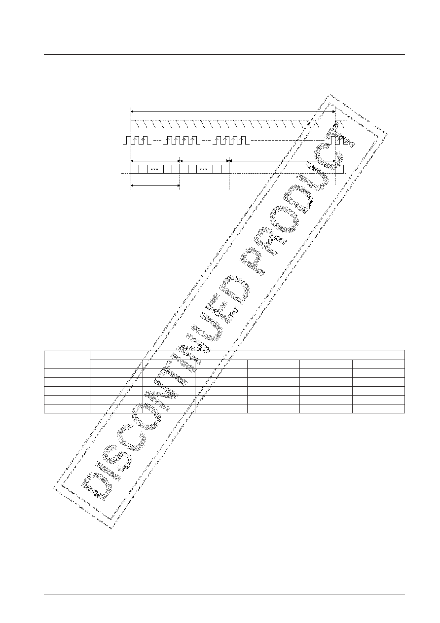
DSP Late Mode
In DSP late mode, the first bit is sampled on the BCKIN rising edge on which the LRCIN low to high transition was
detected. BCKIN edges are not allowed between data words. The word order is left channel first, right channel second.
Audio Data Sampling Rate
The LC708728V master clock supports audio sampling rates from 128 to 768 fs. Here, fs is the audio data sampling rate
(LRCIN), and is one of 32, 44.1, 48, 96, or 128 kHz. In this IC, the internal digital filter and noise shaper circuits are
operated using the master clock.
This IC includes a master clock detection circuit that automatically detects the relationship between the master clock
frequency and the sampling rate. Although this detection circuit automatically corrects if the error is within ±32 clock
cycles, if an error of over ±32 clock cycles occurs, D/A converter operation is stopped and the output is muted
automatically.
We recommend that the master clock be synchronized with LRCIN. Also note that phase differences and jitter with
respect to this clock are allowed. See table 1 for details.
Hardware DSD Mode
DSD mode is set up by setting the MODE pin low and the SCKDSD pin high. In this mode, the built-in digital filters are
bypassed and the bit stream data is supplied to the D/A converters directly. The data converted by the D/A converters
passes through internal low-pass filters and is then output. See figures 27 to 30 for details.
Two data transfer formats are supported: monophase and biphase.
In monophase mode, the DSD data is directly sampled after the rising edge of the 64fs MCLK signal.
In biphase mode, data is supplied in a Manchester encoded format. In Manchester encoding, a bit transition occurs at
every data bit. As a result, corruption of the analog output due to spectral energy is held to an absolute minimum. Based
on a 128 fs clock signal input to the BCKIN pin, data is sampled on the BCKIN signal falling edge when MCLK is low.
See figures 4 and 5 for details.
LRCIN
BCKIN
DIN
Input Word Length (IWL)
1/fs
LEFT CHANNEL
n
2
1
n-1
LSB
MSB
n
2
1
n-1
RIGHT CHANNEL
NO VALID DATA
1
Figure 12 DSP Late Mode Timing Chart
Table 1 Master Clock Frequency vs. Sampling Rate
Sampling rate
Master clock frequency (MHz) (MCLK)
(LRCIN)
128 fs
192 fs
256 fs
384 fs
512 fs
768 fs
32 kHz
4.096
6.144
8.192
12.288
16.384
24.576
44.1 kHz
5.6448
8.467
11.2896
16.9340
22.5792
33.8688
48 kHz
6.114
9.216
12.288
18.432
24.576
36.864
96 kHz
12.288
18.432
24.576
36.864
None
192 kHz
24.576
36.864
None
相关PDF资料 |
PDF描述 |
|---|---|
| LC7137 | PLL FREQUENCY SYNTHESIZER, 20 MHz, PDIP20 |
| LC7131 | PLL FREQUENCY SYNTHESIZER, 20 MHz, PDIP20 |
| LC7232-8291 | SPECIALTY CONSUMER CIRCUIT, PQFP80 |
| LC7232N-8819 | SPECIALTY CONSUMER CIRCUIT, PQFP80 |
| LC7454A | SPECIALTY CONSUMER CIRCUIT, PDIP18 |
相关代理商/技术参数 |
参数描述 |
|---|---|
| LC709004AMJ-AH | 功能描述:接口-I/O扩展器 RoHS:否 制造商:NXP Semiconductors 逻辑系列: 输入/输出端数量: 最大工作频率:100 kHz 工作电源电压:1.65 V to 5.5 V 工作温度范围:- 40 C to + 85 C 安装风格:SMD/SMT 封装 / 箱体:HVQFN-16 封装:Reel |
| LC709006A-E | 功能描述:接口-I/O扩展器 RoHS:否 制造商:NXP Semiconductors 逻辑系列: 输入/输出端数量: 最大工作频率:100 kHz 工作电源电压:1.65 V to 5.5 V 工作温度范围:- 40 C to + 85 C 安装风格:SMD/SMT 封装 / 箱体:HVQFN-16 封装:Reel |
| LC709006A-TLM-E | 功能描述:接口-I/O扩展器 RoHS:否 制造商:NXP Semiconductors 逻辑系列: 输入/输出端数量: 最大工作频率:100 kHz 工作电源电压:1.65 V to 5.5 V 工作温度范围:- 40 C to + 85 C 安装风格:SMD/SMT 封装 / 箱体:HVQFN-16 封装:Reel |
| LC709006V-E | 制造商:ON Semiconductor 功能描述:IO EXPANDER - Ammo Pack 制造商:ON Semiconductor 功能描述:FNFLD / IO EXPANDER |
| LC709006V-TLM-E | 功能描述:接口-I/O扩展器 RoHS:否 制造商:NXP Semiconductors 逻辑系列: 输入/输出端数量: 最大工作频率:100 kHz 工作电源电压:1.65 V to 5.5 V 工作温度范围:- 40 C to + 85 C 安装风格:SMD/SMT 封装 / 箱体:HVQFN-16 封装:Reel |
发布紧急采购,3分钟左右您将得到回复。