- 您现在的位置:买卖IC网 > PDF目录39192 > LC89052T SPECIALTY CONSUMER CIRCUIT, PDSO24 PDF资料下载
参数资料
| 型号: | LC89052T |
| 元件分类: | 消费家电 |
| 英文描述: | SPECIALTY CONSUMER CIRCUIT, PDSO24 |
| 封装: | 0.225 INCH, TSSOP-24 |
| 文件页数: | 33/42页 |
| 文件大小: | 482K |
| 代理商: | LC89052T |
第1页第2页第3页第4页第5页第6页第7页第8页第9页第10页第11页第12页第13页第14页第15页第16页第17页第18页第19页第20页第21页第22页第23页第24页第25页第26页第27页第28页第29页第30页第31页第32页当前第33页第34页第35页第36页第37页第38页第39页第40页第41页第42页
LC89052T
No.7457-39/42
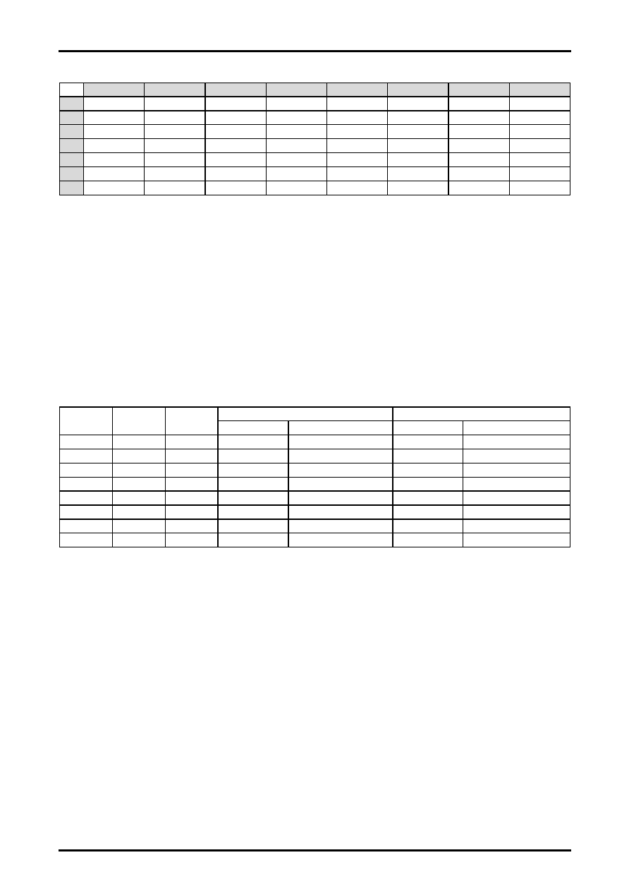
Table 9.10 Output Register: Input fs Calculation Result and Channel Status Data (0xEC)
DO7
DO6
DO5
DO4
DO3
DO2
DO1
DO0
0
FSCAL2
FSCAL1
FSCAL0
0
OUTPCM
OUTERR
0
8
Bit 7
Bit 6
Bit 5
Bit 4
Bit 3
Bit 2
Bit 1
Bit 0
16
Bit 15
Bit 14
Bit 13
Bit 12
Bit 11
Bit 10
Bit 9
Bit 8
24
Bit 23
Bit 22
Bit 21
Bit 20
Bit 19
Bit 18
Bit 17
Bit 16
32
Bit 31
Bit 30
Bit 29
Bit 28
Bit 27
Bit 26
Bit 25
Bit 24
40
Bit 39
Bit 38
Bit 37
Bit 36
Bit 35
Bit 34
Bit 33
Bit 32
48
Bit 47
Bit 46
Bit 45
Bit 44
Bit 43
Bit 42
Bit 41
Bit 40
The error information, non-PCM information, input fs calculation result, and channel status data can be read from this
register. Note that the error information and the non-PCM data information are identical to those at 0xEB.
OUTERR:
ERROR output (Outputs the read-time state.)
0: No transmission error in the PLL locked state
1: Either a transmission error occurred or the PLL circuit is in the unlocked state.
OUTPCM:
____________
AUDIO output (Outputs the read-time state.)
0: Non-PCM signal not detected.
1: Non-PCM signal detected.
The input data fs calculation results are allocated as follows. The target calculation frequency differs depending on the
FS4XIN setting. The calculation range also differs slightly depending on the XIN clock frequency.
Table 9.11 Input fs Calculation Result (Ta = 25°C, VDD = 3.3V, XIN = 11.2896MHz)
FS4XIN = 0
FS4XIN = 1
FSCAL2
FSCAL1
FSCAL0
Target fs
Calculated range
Target fs
Calculated range
0
Out of range
—
Out of range
—
0
1
32kHz
30.9k to 33.2kHz
64kHz
62.0k to 66.4kHz
0
1
0
44.1kHz
42.5k to 45.8kHz
88.2kHz
85.5k to 91.0kHz
0
1
48kHz
46.3k to 49.9kHz
96kHz
92.6k to 99.0kHz
1
0
64kHz
62.1k to 66.4kHz
128kHz
124.0k to 132.8kHz
1
0
1
88.2kHz
85.6k to 91.0kHz
176.4kHz
171.0k to 182.2kHz
1
0
96kHz
92.6k to 99.0kHz
192kHz
185.1k to 198.0kHz
1
—
The first 48 bits of channel status can be read.
Since the channel status consists of 192 frames, updated data can always be read by reading at the interval 192 times
the period of the input sampling frequency.
It is also possible to read by using the updated flag of the interrupt source and setting E/INT to interrupt output to
reduce the load of the microcontroller. This flag is output when the first 48 bits of the current data is compared with
the data of the previous block and found that those data are identical.
相关PDF资料 |
PDF描述 |
|---|---|
| LC89060M | PARALLEL, WORD INPUT LOADING, 6-BIT DAC, PDSO20 |
| LC89060 | PARALLEL, WORD INPUT LOADING, 6-BIT DAC, PDIP16 |
| LC89066 | 1-CH 6-BIT FLASH METHOD ADC, PARALLEL ACCESS, PDIP16 |
| LC89066M | 1-CH 6-BIT FLASH METHOD ADC, PARALLEL ACCESS, PDSO20 |
| LC89080 | TRIPLE, PARALLEL, 8 BITS INPUT LOADING, 8-BIT DAC, PDIP42 |
相关代理商/技术参数 |
参数描述 |
|---|---|
| LC89052TA-E | 功能描述:音频发送器、接收器、收发器 RoHS:否 制造商:Cirrus Logic 工作电源电压:3.3 V, 5 V 电源电流:11.8 mA 通道数量:1 最大工作温度:+ 70 C 接口类型:I2C, SPI 安装风格:SMD/SMT 封装 / 箱体:TSSOP-28 封装: |
| LC89052TA-TLM-E | 功能描述:音频发送器、接收器、收发器 RoHS:否 制造商:Cirrus Logic 工作电源电压:3.3 V, 5 V 电源电流:11.8 mA 通道数量:1 最大工作温度:+ 70 C 接口类型:I2C, SPI 安装风格:SMD/SMT 封装 / 箱体:TSSOP-28 封装: |
| LC89052THS-E | 制造商:ON Semiconductor 功能描述:AUDIO I/F RECEIVER |
| LC890561W | 制造商:SANYO 制造商全称:Sanyo Semicon Device 功能描述:CMOS IC Digital Audio Interface Receiver with Built-in Data Buffer Memory |
| LC890561W-E | 功能描述:音频发送器、接收器、收发器 RoHS:否 制造商:Cirrus Logic 工作电源电压:3.3 V, 5 V 电源电流:11.8 mA 通道数量:1 最大工作温度:+ 70 C 接口类型:I2C, SPI 安装风格:SMD/SMT 封装 / 箱体:TSSOP-28 封装: |
发布紧急采购,3分钟左右您将得到回复。