- 您现在的位置:买卖IC网 > PDF目录39192 > LC89052T SPECIALTY CONSUMER CIRCUIT, PDSO24 PDF资料下载
参数资料
| 型号: | LC89052T |
| 元件分类: | 消费家电 |
| 英文描述: | SPECIALTY CONSUMER CIRCUIT, PDSO24 |
| 封装: | 0.225 INCH, TSSOP-24 |
| 文件页数: | 5/42页 |
| 文件大小: | 482K |
| 代理商: | LC89052T |
第1页第2页第3页第4页当前第5页第6页第7页第8页第9页第10页第11页第12页第13页第14页第15页第16页第17页第18页第19页第20页第21页第22页第23页第24页第25页第26页第27页第28页第29页第30页第31页第32页第33页第34页第35页第36页第37页第38页第39页第40页第41页第42页
LC89052T
No.7457-13/42
8.3.3 Output clocks (CKOUT, BCK, LRCK)
The clock source for the clocks output from CKOUT, BCK, and LRCK can be selected from two master clocks, the
PLL circuit and the XIN pin.
Normally, when the PLL circuit is locked, the master clock is switched to the PLL source, and when the PLL circuit is
unlocked, the master clock automatically switches to the XIN source. To switch the clock source forcibly, set with
OCKSEL. Clock continuity is maintained when the clock source is selected by the locked/unlocked state of the PLL
circuit or OCKSEL.
Clock switching depends on the PLL circuit locked/unlocked state at the time of the register setup. If the PLL source
is selected with OCKSEL when the PLL circuit is unlocked, the clock is automatically switched after the PLL circuit
is locked.
When VCO operation is stopped with PLLOPR, XIN becomes the clock source. However, clock continuity cannot be
maintained if the operation is stopped with PLLOPR while the PLL circuit is locked. When a low-power mode is set,
continuity cannot be maintained if the mode is switched from the locked PLL.
Table 8.4 Register Settings, PLL States, and the Clock Source
OCKSEL
0
1
PLL state
Locked
Unlocked
Locked
Unlocked
Clock source
PLL
XIN
Either the PLL clock or the XIN clock is output from the CKOUT pin. The divided clock of CKOUT is output from
the BCK pin and LRCK pin.
The PLL lock time frequency is set with PLLCK[1:0]. However, it is possible to maintain clock continuity without
losing the PLL locked state when switching, in the PLL locked state, from the 512fs setting mode with PLLCK[1:0] =
"10" to the (512/2)fs setting with the PLLCK[1:0] = "11", as well as when switching in the reverse direction.
If you use the following procedure to switch between 512fs and (512/2)fs, the BCK and LRCK output clock
continuity can be maintained, and the CKOUT output clock frequency can be held within a narrow band. Other
PLLCK[1:0] switching would result in a lock error.
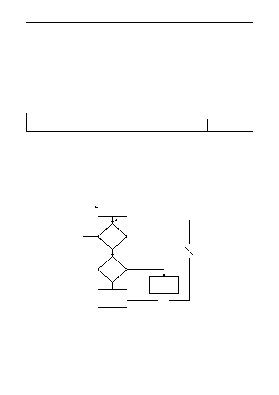
Figure 8.4 Flowchart for CKOUT Output Clock Narrow Band Operation
Data input
LOCK
detection
fs
calculation
512fs set
PLLCK0=0
PLLCK1=1
PLLCK0=1
PLLCK1=1
No
Yes
fs=96kHz
fs=48kHz
(512/2)fs set
CKOUT output
24.576MHz
相关PDF资料 |
PDF描述 |
|---|---|
| LC89060M | PARALLEL, WORD INPUT LOADING, 6-BIT DAC, PDSO20 |
| LC89060 | PARALLEL, WORD INPUT LOADING, 6-BIT DAC, PDIP16 |
| LC89066 | 1-CH 6-BIT FLASH METHOD ADC, PARALLEL ACCESS, PDIP16 |
| LC89066M | 1-CH 6-BIT FLASH METHOD ADC, PARALLEL ACCESS, PDSO20 |
| LC89080 | TRIPLE, PARALLEL, 8 BITS INPUT LOADING, 8-BIT DAC, PDIP42 |
相关代理商/技术参数 |
参数描述 |
|---|---|
| LC89052TA-E | 功能描述:音频发送器、接收器、收发器 RoHS:否 制造商:Cirrus Logic 工作电源电压:3.3 V, 5 V 电源电流:11.8 mA 通道数量:1 最大工作温度:+ 70 C 接口类型:I2C, SPI 安装风格:SMD/SMT 封装 / 箱体:TSSOP-28 封装: |
| LC89052TA-TLM-E | 功能描述:音频发送器、接收器、收发器 RoHS:否 制造商:Cirrus Logic 工作电源电压:3.3 V, 5 V 电源电流:11.8 mA 通道数量:1 最大工作温度:+ 70 C 接口类型:I2C, SPI 安装风格:SMD/SMT 封装 / 箱体:TSSOP-28 封装: |
| LC89052THS-E | 制造商:ON Semiconductor 功能描述:AUDIO I/F RECEIVER |
| LC890561W | 制造商:SANYO 制造商全称:Sanyo Semicon Device 功能描述:CMOS IC Digital Audio Interface Receiver with Built-in Data Buffer Memory |
| LC890561W-E | 功能描述:音频发送器、接收器、收发器 RoHS:否 制造商:Cirrus Logic 工作电源电压:3.3 V, 5 V 电源电流:11.8 mA 通道数量:1 最大工作温度:+ 70 C 接口类型:I2C, SPI 安装风格:SMD/SMT 封装 / 箱体:TSSOP-28 封装: |
发布紧急采购,3分钟左右您将得到回复。