- 您现在的位置:买卖IC网 > PDF目录39192 > LC89052T SPECIALTY CONSUMER CIRCUIT, PDSO24 PDF资料下载
参数资料
| 型号: | LC89052T |
| 元件分类: | 消费家电 |
| 英文描述: | SPECIALTY CONSUMER CIRCUIT, PDSO24 |
| 封装: | 0.225 INCH, TSSOP-24 |
| 文件页数: | 7/42页 |
| 文件大小: | 482K |
| 代理商: | LC89052T |
第1页第2页第3页第4页第5页第6页当前第7页第8页第9页第10页第11页第12页第13页第14页第15页第16页第17页第18页第19页第20页第21页第22页第23页第24页第25页第26页第27页第28页第29页第30页第31页第32页第33页第34页第35页第36页第37页第38页第39页第40页第41页第42页
LC89052T
No.7457-15/42
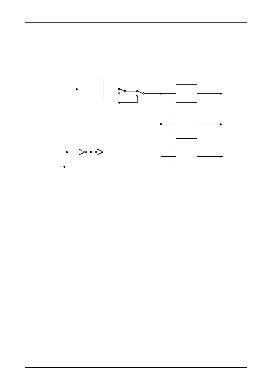
8.3.4 Clock system diagram
This section shows the relationship between the two types of master clock and clock switching and dividing functions.
The items in square brackets near the switch and function blocks are the names of write commands.
Lock/Unlock is switched automatically according to the PLL lock/unlock state.
Figure 8.5 Master Clock System Diagram
8.3.5 Point to notice when switching the clock source
If an attempt is made to switch the clock source from PLL lock state (oscillator amplifier stopped) to XIN using
OCKSEL when a mode in which the results of input fs calculation are reflected in the error flags is specified through
FLIMIT, an error signal (H) is temporarily placed at the ERROR pin though the continuity of the clock is preserved.
The reason for this follows. When the clock switching is carried out, the oscillator amplifier is activated and the input
fs calculation is restarted. At the same time, the old results of fs calculation are reset and consequently, a change in
the fs value is recognized when the old fs value is compared with the newly calculated fs value.
To switch the clock source using OCKSEL while maintaining the state of the ERROR pin when the PLL is locked in
this mode setting, it is necessary to put the oscillator amplifier into the continuous mode using AMPCNT.
Note that when the clock source is switched to XIN from the state where the oscillator amplifier is stopped with the
PLL circuit locked, output clocks whose source is XIN start outputting after the oscillator amplifier has started
operation. While the PLL is locked, clock source switching from XIN to PLL is carried out immediately. In both
cases, clock continuity is maintained.
When the CKOUT clock is supplied to XIN without using an oscillator or an external clock, the VCO free-running
frequency output from the CKOUT pin with the PLL unlocked is somewhere between 10M and 16MHz. Clock
signals created by dividing CKOUT are output from BCK and LRCK pins. However, these clock frequencies vary
depending on the LC89052T sample and fluctuate depending on supply voltage and operating environments.
Therefore, the frequency is not fixed. You need to take care when using the CKOUT, BCK, and LRCK clocks while
the PLL circuit is unlocked.
RXIN
Lock/Unlock
[OCKSEL]
Divider
1/2
Divider
1/256
CKOUT
BCK
LRCK
XIN
XOUT
PLL
(256fs)
[PLLCK0]
[XISEL0]
(384fs)
[PLLOPR]
[AMPCNT]
1/3
1/384
[XINSET]
[AMPOPR]
[XISEL1]
[PLLCK1]
[XISEL2]
(512fs)
1/512
(512/2fs)
Divider
1/2
[MCKHFO]
1/4
1/6
1/8
相关PDF资料 |
PDF描述 |
|---|---|
| LC89060M | PARALLEL, WORD INPUT LOADING, 6-BIT DAC, PDSO20 |
| LC89060 | PARALLEL, WORD INPUT LOADING, 6-BIT DAC, PDIP16 |
| LC89066 | 1-CH 6-BIT FLASH METHOD ADC, PARALLEL ACCESS, PDIP16 |
| LC89066M | 1-CH 6-BIT FLASH METHOD ADC, PARALLEL ACCESS, PDSO20 |
| LC89080 | TRIPLE, PARALLEL, 8 BITS INPUT LOADING, 8-BIT DAC, PDIP42 |
相关代理商/技术参数 |
参数描述 |
|---|---|
| LC89052TA-E | 功能描述:音频发送器、接收器、收发器 RoHS:否 制造商:Cirrus Logic 工作电源电压:3.3 V, 5 V 电源电流:11.8 mA 通道数量:1 最大工作温度:+ 70 C 接口类型:I2C, SPI 安装风格:SMD/SMT 封装 / 箱体:TSSOP-28 封装: |
| LC89052TA-TLM-E | 功能描述:音频发送器、接收器、收发器 RoHS:否 制造商:Cirrus Logic 工作电源电压:3.3 V, 5 V 电源电流:11.8 mA 通道数量:1 最大工作温度:+ 70 C 接口类型:I2C, SPI 安装风格:SMD/SMT 封装 / 箱体:TSSOP-28 封装: |
| LC89052THS-E | 制造商:ON Semiconductor 功能描述:AUDIO I/F RECEIVER |
| LC890561W | 制造商:SANYO 制造商全称:Sanyo Semicon Device 功能描述:CMOS IC Digital Audio Interface Receiver with Built-in Data Buffer Memory |
| LC890561W-E | 功能描述:音频发送器、接收器、收发器 RoHS:否 制造商:Cirrus Logic 工作电源电压:3.3 V, 5 V 电源电流:11.8 mA 通道数量:1 最大工作温度:+ 70 C 接口类型:I2C, SPI 安装风格:SMD/SMT 封装 / 箱体:TSSOP-28 封装: |
发布紧急采购,3分钟左右您将得到回复。