- 您现在的位置:买卖IC网 > PDF目录19858 > LCMXO1200C-5FTN256C (Lattice Semiconductor Corporation)IC PLD 1200LUTS 211I/O 256-BGA PDF资料下载
参数资料
| 型号: | LCMXO1200C-5FTN256C |
| 厂商: | Lattice Semiconductor Corporation |
| 文件页数: | 12/88页 |
| 文件大小: | 0K |
| 描述: | IC PLD 1200LUTS 211I/O 256-BGA |
| 标准包装: | 90 |
| 系列: | MachXO |
| 可编程类型: | 系统内可编程 |
| 最大延迟时间 tpd(1): | 3.6ns |
| 电压电源 - 内部: | 1.71 V ~ 3.465 V |
| 宏单元数: | 600 |
| 输入/输出数: | 211 |
| 工作温度: | 0°C ~ 85°C |
| 安装类型: | 表面贴装 |
| 封装/外壳: | 256-LBGA |
| 供应商设备封装: | 256-FTBGA(17x17) |
| 包装: | 托盘 |
| 其它名称: | 220-1180 |
第1页第2页第3页第4页第5页第6页第7页第8页第9页第10页第11页当前第12页第13页第14页第15页第16页第17页第18页第19页第20页第21页第22页第23页第24页第25页第26页第27页第28页第29页第30页第31页第32页第33页第34页第35页第36页第37页第38页第39页第40页第41页第42页第43页第44页第45页第46页第47页第48页第49页第50页第51页第52页第53页第54页第55页第56页第57页第58页第59页第60页第61页第62页第63页第64页第65页第66页第67页第68页第69页第70页第71页第72页第73页第74页第75页第76页第77页第78页第79页第80页第81页第82页第83页第84页第85页第86页第87页第88页
�� �
�
�Architecture�
�MachXO� Family� Data� Sheet�
�sysCLOCK� Phase� Locked� Loops� (PLLs)�
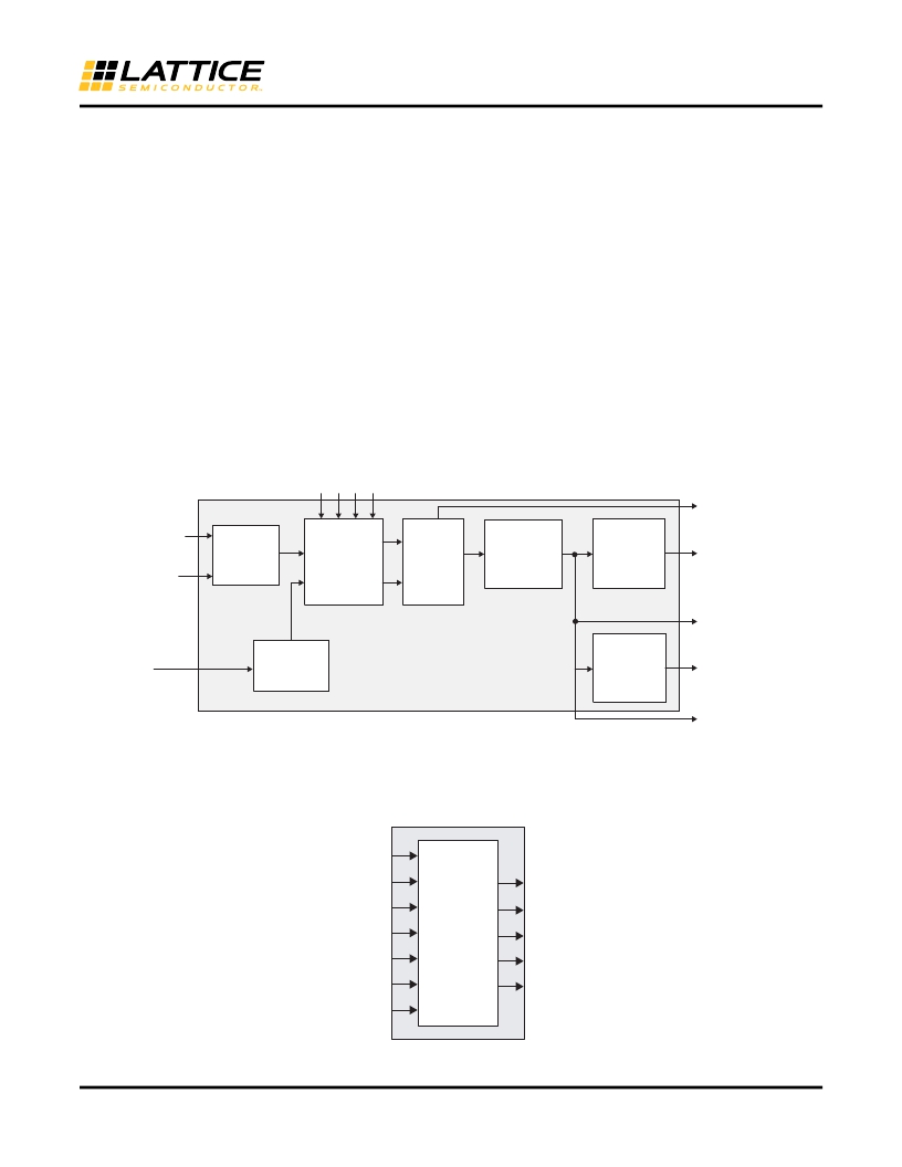
�The� MachXO1200� and� MachXO2280� provide� PLL� support.� The� source� of� the� PLL� input� divider� can� come� from� an�
�external� pin� or� from� internal� routing.� There� are� four� sources� of� feedback� signals� to� the� feedback� divider:� from�
�CLKINTFB� (internal� feedback� port),� from� the� global� clock� nets,� from� the� output� of� the� post� scalar� divider,� and� from�
�the� routing� (or� from� an� external� pin).� There� is� a� PLL_LOCK� signal� to� indicate� that� the� PLL� has� locked� on� to� the� input�
�clock� signal.� Figure� 2-10� shows� the� sysCLOCK� PLL� diagram.�
�The� setup� and� hold� times� of� the� device� can� be� improved� by� programming� a� delay� in� the� feedback� or� input� path� of�
�the� PLL� which� will� advance� or� delay� the� output� clock� with� reference� to� the� input� clock.� This� delay� can� be� either� pro-�
�grammed� during� configuration� or� can� be� adjusted� dynamically.� In� dynamic� mode,� the� PLL� may� lose� lock� after�
�adjustment� and� not� relock� until� the� t� LOCK� parameter� has� been� satisfied.� Additionally,� the� phase� and� duty� cycle� block�
�allows� the� user� to� adjust� the� phase� and� duty� cycle� of� the� CLKOS� output.�
�The� sysCLOCK� PLLs� provide� the� ability� to� synthesize� clock� frequencies.� Each� PLL� has� four� dividers� associated�
�with� it:� input� clock� divider,� feedback� divider,� post� scalar� divider,� and� secondary� clock� divider.� The� input� clock� divider�
�is� used� to� divide� the� input� clock� signal,� while� the� feedback� divider� is� used� to� multiply� the� input� clock� signal.� The� post�
�scalar� divider� allows� the� VCO� to� operate� at� higher� frequencies� than� the� clock� output,� thereby� increasing� the� fre-�
�quency� range.� The� secondary� divider� is� used� to� derive� lower� frequency� outputs.�
�Figure� 2-10.� PLL� Diagram�
�Dynamic� Delay� Adjustment�
�LOCK�
�RST�
�CLKI�
�(from� routing� or�
�Input� Clock�
�Divider�
�(CLKI)�
�Delay�
�Adjust�
�Voltage�
�VCO�
�Controlled�
�Oscillator�
�Post� Scalar�
�Divider�
�(CLKOP)�
�Phase/Duty�
�Select�
�CLKOS�
�external� pin)�
�CLKOP�
�CLKFB�
�(from� Post� Scalar�
�Divider� output,�
�Feedback�
�Divider�
�(CLKFB)�
�Secondary�
�Clock�
�Divider�
�(CLKOK)�
�CLKOK�
�clock� net,�
�routing/external�
�pin� or� CLKINTFB�
�port�
�CLKINTFB�
�(internal� feedback)�
�Figure� 2-11� shows� the� available� macros� for� the� PLL.� Table� 2-5� provides� signal� description� of� the� PLL� Block.�
�Figure� 2-11.� PLL� Primitive�
�RST�
�CLKI�
�CLKFB�
�CLKOP�
�CLKOS�
�DDA� MODE�
�DDAIZR�
�DDAILAG�
�EHXPLLC�
�CLKOK�
�LOCK�
�CLKINTFB�
�DDAIDEL[2:0]�
�2-9�
�相关PDF资料 |
PDF描述 |
|---|---|
| MAX8559ETAG2+T | IC REG LDO 3V/1.8V .3A 8-TDFN |
| NCP1013AP100G | IC OFFLINE SWITCH SMPS OVP 8DIP |
| VE-2WY-CW-F1 | CONVERTER MOD DC/DC 3.3V 66W |
| GSM08DSUS | CONN EDGECARD 16POS DIP .156 SLD |
| NCP1014AP065G | IC OFFLINE SWIT SMPS CM OVP 8DIP |
相关代理商/技术参数 |
参数描述 |
|---|---|
| LCMXO1200C-5M132C | 功能描述:CPLD - 复杂可编程逻辑器件 1200 LUTs 101 IO 1.8 /2.5/3.3V -5 Spd RoHS:否 制造商:Lattice 系列: 存储类型:EEPROM 大电池数量:128 最大工作频率:333 MHz 延迟时间:2.7 ns 可编程输入/输出端数量:64 工作电源电压:3.3 V 最大工作温度:+ 90 C 最小工作温度:0 C 封装 / 箱体:TQFP-100 |
| LCMXO1200C-5MN132C | 功能描述:CPLD - 复杂可编程逻辑器件 1200 LUTs 101 IO 1.8 /2.5/3.3V -5 Spd RoHS:否 制造商:Lattice 系列: 存储类型:EEPROM 大电池数量:128 最大工作频率:333 MHz 延迟时间:2.7 ns 可编程输入/输出端数量:64 工作电源电压:3.3 V 最大工作温度:+ 90 C 最小工作温度:0 C 封装 / 箱体:TQFP-100 |
| LCMXO1200C-5T100C | 功能描述:CPLD - 复杂可编程逻辑器件 1200 LUTs 73 IO 1.8/ 2.5/3.3V -5 Spd RoHS:否 制造商:Lattice 系列: 存储类型:EEPROM 大电池数量:128 最大工作频率:333 MHz 延迟时间:2.7 ns 可编程输入/输出端数量:64 工作电源电压:3.3 V 最大工作温度:+ 90 C 最小工作温度:0 C 封装 / 箱体:TQFP-100 |
| LCMXO1200C-5T144C | 功能描述:CPLD - 复杂可编程逻辑器件 1200 LUTs 113 IO 1.8 /2.5/3.3V -5 Spd RoHS:否 制造商:Lattice 系列: 存储类型:EEPROM 大电池数量:128 最大工作频率:333 MHz 延迟时间:2.7 ns 可编程输入/输出端数量:64 工作电源电压:3.3 V 最大工作温度:+ 90 C 最小工作温度:0 C 封装 / 箱体:TQFP-100 |
| LCMXO1200C-5TN100C | 功能描述:CPLD - 复杂可编程逻辑器件 1200 LUTS 73 I/O RoHS:否 制造商:Lattice 系列: 存储类型:EEPROM 大电池数量:128 最大工作频率:333 MHz 延迟时间:2.7 ns 可编程输入/输出端数量:64 工作电源电压:3.3 V 最大工作温度:+ 90 C 最小工作温度:0 C 封装 / 箱体:TQFP-100 |
发布紧急采购,3分钟左右您将得到回复。