- 您现在的位置:买卖IC网 > PDF目录19858 > LCMXO1200C-5FTN256C (Lattice Semiconductor Corporation)IC PLD 1200LUTS 211I/O 256-BGA PDF资料下载
参数资料
| 型号: | LCMXO1200C-5FTN256C |
| 厂商: | Lattice Semiconductor Corporation |
| 文件页数: | 6/88页 |
| 文件大小: | 0K |
| 描述: | IC PLD 1200LUTS 211I/O 256-BGA |
| 标准包装: | 90 |
| 系列: | MachXO |
| 可编程类型: | 系统内可编程 |
| 最大延迟时间 tpd(1): | 3.6ns |
| 电压电源 - 内部: | 1.71 V ~ 3.465 V |
| 宏单元数: | 600 |
| 输入/输出数: | 211 |
| 工作温度: | 0°C ~ 85°C |
| 安装类型: | 表面贴装 |
| 封装/外壳: | 256-LBGA |
| 供应商设备封装: | 256-FTBGA(17x17) |
| 包装: | 托盘 |
| 其它名称: | 220-1180 |
第1页第2页第3页第4页第5页当前第6页第7页第8页第9页第10页第11页第12页第13页第14页第15页第16页第17页第18页第19页第20页第21页第22页第23页第24页第25页第26页第27页第28页第29页第30页第31页第32页第33页第34页第35页第36页第37页第38页第39页第40页第41页第42页第43页第44页第45页第46页第47页第48页第49页第50页第51页第52页第53页第54页第55页第56页第57页第58页第59页第60页第61页第62页第63页第64页第65页第66页第67页第68页第69页第70页第71页第72页第73页第74页第75页第76页第77页第78页第79页第80页第81页第82页第83页第84页第85页第86页第87页第88页
�� �
�
�Architecture�
�MachXO� Family� Data� Sheet�
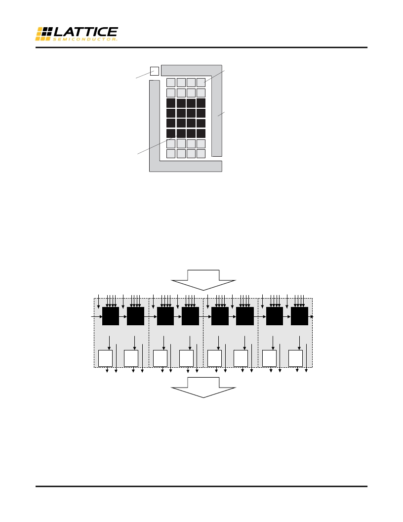
�Figure� 2-3.� Top� View� of� the� MachXO256� Device�
�Programmable� Function�
�JTAG� Port�
�Units� without� RAM� (PFFs)�
�PIOs� Arranged�
�into� sysIO� Banks�
�Programmable�
�Function�
�Units� with�
�RAM� (PFUs)�
�PFU� Blocks�
�The� core� of� the� MachXO� devices� consists� of� PFU� and� PFF� blocks.� The� PFUs� can� be� programmed� to� perform�
�Logic,� Arithmetic,� Distributed� RAM,� and� Distributed� ROM� functions.� PFF� blocks� can� be� programmed� to� perform�
�Logic,� Arithmetic,� and� Distributed� ROM� functions.� Except� where� necessary,� the� remainder� of� this� data� sheet� will�
�use� the� term� PFU� to� refer� to� both� PFU� and� PFF� blocks.�
�Each� PFU� block� consists� of� four� interconnected� Slices,� numbered� 0-3� as� shown� in� Figure� 2-4.� There� are� 53� inputs�
�and� 25� outputs� associated� with� each� PFU� block.�
�Figure� 2-4.� PFU� Diagram�
�From�
�Routing�
�FCIN�
�LUT4� &�
�CARRY�
�LUT4� &�
�CARRY�
�LUT4� &�
�CARRY�
�LUT4� &�
�CARRY�
�LUT4� &�
�CARRY�
�LUT4� &�
�CARRY�
�LUT4� &�
�CARRY�
�LUT4� &�
�CARRY�
�FCO�
�Slice� 0�
�Slice� 1�
�Slice� 2�
�Slice� 3�
�D�
�FF/�
�Latch�
�D�
�FF/�
�Latch�
�D�
�FF/�
�Latch�
�D�
�FF/�
�Latch�
�D�
�FF/�
�Latch�
�D�
�FF/�
�Latch�
�D�
�FF/�
�Latch�
�D�
�FF/�
�Latch�
�To�
�Routing�
�Slice�
�Each� Slice� contains� two� LUT4� lookup� tables� feeding� two� registers� (programmed� to� be� in� FF� or� Latch� mode),� and�
�some� associated� logic� that� allows� the� LUTs� to� be� combined� to� perform� functions� such� as� LUT5,� LUT6,� LUT7,� and�
�LUT8.� There� is� control� logic� to� perform� set/reset� functions� (programmable� as� synchronous/asynchronous),� clock�
�select,� chip-select,� and� wider� RAM/ROM� functions.� Figure� 2-5� shows� an� overview� of� the� internal� logic� of� the� Slice.�
�The� registers� in� the� Slice� can� be� configured� for� positive/negative� and� edge/level� clocks.�
�2-3�
�相关PDF资料 |
PDF描述 |
|---|---|
| MAX8559ETAG2+T | IC REG LDO 3V/1.8V .3A 8-TDFN |
| NCP1013AP100G | IC OFFLINE SWITCH SMPS OVP 8DIP |
| VE-2WY-CW-F1 | CONVERTER MOD DC/DC 3.3V 66W |
| GSM08DSUS | CONN EDGECARD 16POS DIP .156 SLD |
| NCP1014AP065G | IC OFFLINE SWIT SMPS CM OVP 8DIP |
相关代理商/技术参数 |
参数描述 |
|---|---|
| LCMXO1200C-5M132C | 功能描述:CPLD - 复杂可编程逻辑器件 1200 LUTs 101 IO 1.8 /2.5/3.3V -5 Spd RoHS:否 制造商:Lattice 系列: 存储类型:EEPROM 大电池数量:128 最大工作频率:333 MHz 延迟时间:2.7 ns 可编程输入/输出端数量:64 工作电源电压:3.3 V 最大工作温度:+ 90 C 最小工作温度:0 C 封装 / 箱体:TQFP-100 |
| LCMXO1200C-5MN132C | 功能描述:CPLD - 复杂可编程逻辑器件 1200 LUTs 101 IO 1.8 /2.5/3.3V -5 Spd RoHS:否 制造商:Lattice 系列: 存储类型:EEPROM 大电池数量:128 最大工作频率:333 MHz 延迟时间:2.7 ns 可编程输入/输出端数量:64 工作电源电压:3.3 V 最大工作温度:+ 90 C 最小工作温度:0 C 封装 / 箱体:TQFP-100 |
| LCMXO1200C-5T100C | 功能描述:CPLD - 复杂可编程逻辑器件 1200 LUTs 73 IO 1.8/ 2.5/3.3V -5 Spd RoHS:否 制造商:Lattice 系列: 存储类型:EEPROM 大电池数量:128 最大工作频率:333 MHz 延迟时间:2.7 ns 可编程输入/输出端数量:64 工作电源电压:3.3 V 最大工作温度:+ 90 C 最小工作温度:0 C 封装 / 箱体:TQFP-100 |
| LCMXO1200C-5T144C | 功能描述:CPLD - 复杂可编程逻辑器件 1200 LUTs 113 IO 1.8 /2.5/3.3V -5 Spd RoHS:否 制造商:Lattice 系列: 存储类型:EEPROM 大电池数量:128 最大工作频率:333 MHz 延迟时间:2.7 ns 可编程输入/输出端数量:64 工作电源电压:3.3 V 最大工作温度:+ 90 C 最小工作温度:0 C 封装 / 箱体:TQFP-100 |
| LCMXO1200C-5TN100C | 功能描述:CPLD - 复杂可编程逻辑器件 1200 LUTS 73 I/O RoHS:否 制造商:Lattice 系列: 存储类型:EEPROM 大电池数量:128 最大工作频率:333 MHz 延迟时间:2.7 ns 可编程输入/输出端数量:64 工作电源电压:3.3 V 最大工作温度:+ 90 C 最小工作温度:0 C 封装 / 箱体:TQFP-100 |
发布紧急采购,3分钟左右您将得到回复。