- 您现在的位置:买卖IC网 > PDF目录17108 > LFXP10C-L-EV (Lattice Semiconductor Corporation)BOARD EVAL LATTICEXP10C STD PDF资料下载
参数资料
| 型号: | LFXP10C-L-EV |
| 厂商: | Lattice Semiconductor Corporation |
| 文件页数: | 11/20页 |
| 文件大小: | 0K |
| 描述: | BOARD EVAL LATTICEXP10C STD |
| 标准包装: | 1 |
| 系列: | XP |
| 类型: | FPGA |
| 适用于相关产品: | LFXP10C |
| 所含物品: | 板 |
| 其它名称: | LFXP10CLEV |
�� �
�
�LatticeXP� Standard� Evaluation� Board�
�Lattice� Semiconductor�
�User’s� Guide�
�Programming� Headers�
�Two� programming� headers� are� provided� on� the� evaluation� board,� providing� access� to� the� LatticeXP� JTAG� port.�
�Both� 1x10� and� 2x5� formats� are� available� for� compatibility� with� all� Lattice� ispDOWNLOAD� ?� cables.� The� pinouts� for�
�the� headers� are� provided� in� Tables� 6� and� 7.�
�Important� Note:� The� board� must� be� un-powered� when� connecting,� disconnecting,� or� reconnecting� the� ispDOWN-�
�LOAD� Cable.� Always� connect� the� ispDOWNLOAD� Cable's� GND� pin� (black� wire),� before� connecting� any� other� JTAG�
�pins.� Failure� to� follow� these� procedures� can� in� result� in� damage� to� the� LatticeXP� FPGA� device� and� render� the�
�board� inoperable.�
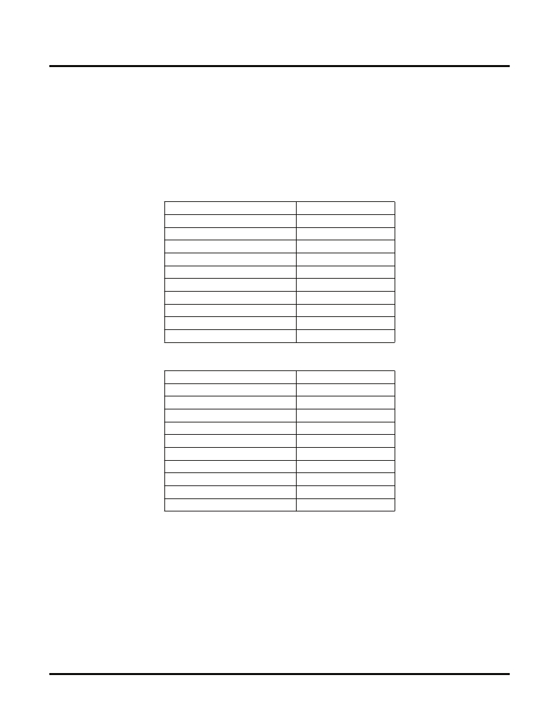
�Table� 7.� JTAG� Programming� Headers� Function� JP8� (2x5)�
�JTAG� Programming� Function�
�TCK�
�GND�
�TMS�
�GND�
�TDI�
�VCC� (3.3V)�
�TDO�
�GND�
�TRST�
�PROGRAM�
�Table� 8.� JTAG� Programming� Headers� Function� JP7� (1x10)�
�JTAG� Programming� Function�
�VCC� (3.3V)�
�TDO�
�TDI�
�PROGRAM�
�TRST�
�TMS�
�GND�
�TCK�
�DONE�
�INIT�
�JP8� Pin� Number� (2x5)�
�1�
�2�
�3�
�4�
�5�
�6�
�7�
�8�
�9�
�10�
�JP7� Pin� Number� (1x10)�
�1�
�2�
�3�
�4�
�5�
�6�
�7�
�8�
�9�
�10�
�Power� Supply�
�Power� can� be� supplied� to� the� LatticeXP� Standard� Evaluation� Board� via� the� banana� jacks� (J1,� 2,� 5,� 6� –� all� PCB� revi-�
�sions),� or� a� coaxial� DC� connector� (J3� –� Rev.� B� PCB� only),� which� receive� power� from� either� a� bench� power� supply� or�
�a� brick� style� power� supply.�
�[Rev.� B� Only]� The� output� from� the� DC� system� is� controlled� by� switch� SW1.� This� is� a� small� surface� mount� switch� that�
�enables� and� disables� the� LTC1775� DC-DC� conversion� chip.� The� output� voltages� from� the� power� supply� are� enabled�
�when� the� switch� is� in� the� left� position.�
�[Rev.� B� Only]� The� 5.0V� to� 28.0V� DC� input� voltage� (input� to� either� J2� or� J3)� is� converted� by� DC-DC� converters� and�
�switching� power� supplies� to� provide� 3.3V,� 1.2V,� and� an� adjustable� DC� source� on� the� board.� The� output� from� these�
�11�
�相关PDF资料 |
PDF描述 |
|---|---|
| ECM18DTAS | CONN EDGECARD 36POS R/A .156 SLD |
| AT91SAM7X-EK | KIT EVAL FOR AT91SAM7X256/128 |
| AIRD-03-392K | INDUCTOR PWR DRUM CORE 3900UH |
| UVZ2E101MHD | CAP ALUM 100UF 250V 20% RADIAL |
| UVR1J222MHD | CAP ALUM 2200UF 63V 20% RADIAL |
相关代理商/技术参数 |
参数描述 |
|---|---|
| LFXP10E-3F256C | 功能描述:FPGA - 现场可编程门阵列 9.7K LUTs 188 IO 1.2 V -3 Spd RoHS:否 制造商:Altera Corporation 系列:Cyclone V E 栅极数量: 逻辑块数量:943 内嵌式块RAM - EBR:1956 kbit 输入/输出端数量:128 最大工作频率:800 MHz 工作电源电压:1.1 V 最大工作温度:+ 70 C 安装风格:SMD/SMT 封装 / 箱体:FBGA-256 |
| LFXP10E-3F256CES | 功能描述:FPGA - 现场可编程门阵列 RoHS:否 制造商:Altera Corporation 系列:Cyclone V E 栅极数量: 逻辑块数量:943 内嵌式块RAM - EBR:1956 kbit 输入/输出端数量:128 最大工作频率:800 MHz 工作电源电压:1.1 V 最大工作温度:+ 70 C 安装风格:SMD/SMT 封装 / 箱体:FBGA-256 |
| LFXP10E-3F256I | 功能描述:FPGA - 现场可编程门阵列 9.7K LUTs 188 I/O 1.2V -3 Speed IND RoHS:否 制造商:Altera Corporation 系列:Cyclone V E 栅极数量: 逻辑块数量:943 内嵌式块RAM - EBR:1956 kbit 输入/输出端数量:128 最大工作频率:800 MHz 工作电源电压:1.1 V 最大工作温度:+ 70 C 安装风格:SMD/SMT 封装 / 箱体:FBGA-256 |
| LFXP10E-3F256IES | 功能描述:FPGA - 现场可编程门阵列 9.7K LUTs 188 I/O 1.2V -3 Speed IND RoHS:否 制造商:Altera Corporation 系列:Cyclone V E 栅极数量: 逻辑块数量:943 内嵌式块RAM - EBR:1956 kbit 输入/输出端数量:128 最大工作频率:800 MHz 工作电源电压:1.1 V 最大工作温度:+ 70 C 安装风格:SMD/SMT 封装 / 箱体:FBGA-256 |
| LFXP10E-3F388C | 功能描述:FPGA - 现场可编程门阵列 9.7K LUTs 244 IO 1.2 V -3 Spd RoHS:否 制造商:Altera Corporation 系列:Cyclone V E 栅极数量: 逻辑块数量:943 内嵌式块RAM - EBR:1956 kbit 输入/输出端数量:128 最大工作频率:800 MHz 工作电源电压:1.1 V 最大工作温度:+ 70 C 安装风格:SMD/SMT 封装 / 箱体:FBGA-256 |
发布紧急采购,3分钟左右您将得到回复。