- 您现在的位置:买卖IC网 > PDF目录4590 > LFXP6E-3FN256I (Lattice Semiconductor Corporation)IC FPGA 5.8KLUTS 188I/O 256-BGA PDF资料下载
参数资料
| 型号: | LFXP6E-3FN256I |
| 厂商: | Lattice Semiconductor Corporation |
| 文件页数: | 240/397页 |
| 文件大小: | 0K |
| 描述: | IC FPGA 5.8KLUTS 188I/O 256-BGA |
| 标准包装: | 90 |
| 系列: | XP |
| 逻辑元件/单元数: | 6000 |
| RAM 位总计: | 73728 |
| 输入/输出数: | 188 |
| 电源电压: | 1.14 V ~ 1.26 V |
| 安装类型: | 表面贴装 |
| 工作温度: | -40°C ~ 100°C |
| 封装/外壳: | 256-BGA |
| 供应商设备封装: | 256-FPBGA(17x17) |
第1页第2页第3页第4页第5页第6页第7页第8页第9页第10页第11页第12页第13页第14页第15页第16页第17页第18页第19页第20页第21页第22页第23页第24页第25页第26页第27页第28页第29页第30页第31页第32页第33页第34页第35页第36页第37页第38页第39页第40页第41页第42页第43页第44页第45页第46页第47页第48页第49页第50页第51页第52页第53页第54页第55页第56页第57页第58页第59页第60页第61页第62页第63页第64页第65页第66页第67页第68页第69页第70页第71页第72页第73页第74页第75页第76页第77页第78页第79页第80页第81页第82页第83页第84页第85页第86页第87页第88页第89页第90页第91页第92页第93页第94页第95页第96页第97页第98页第99页第100页第101页第102页第103页第104页第105页第106页第107页第108页第109页第110页第111页第112页第113页第114页第115页第116页第117页第118页第119页第120页第121页第122页第123页第124页第125页第126页第127页第128页第129页第130页第131页第132页第133页第134页第135页第136页第137页第138页第139页第140页第141页第142页第143页第144页第145页第146页第147页第148页第149页第150页第151页第152页第153页第154页第155页第156页第157页第158页第159页第160页第161页第162页第163页第164页第165页第166页第167页第168页第169页第170页第171页第172页第173页第174页第175页第176页第177页第178页第179页第180页第181页第182页第183页第184页第185页第186页第187页第188页第189页第190页第191页第192页第193页第194页第195页第196页第197页第198页第199页第200页第201页第202页第203页第204页第205页第206页第207页第208页第209页第210页第211页第212页第213页第214页第215页第216页第217页第218页第219页第220页第221页第222页第223页第224页第225页第226页第227页第228页第229页第230页第231页第232页第233页第234页第235页第236页第237页第238页第239页当前第240页第241页第242页第243页第244页第245页第246页第247页第248页第249页第250页第251页第252页第253页第254页第255页第256页第257页第258页第259页第260页第261页第262页第263页第264页第265页第266页第267页第268页第269页第270页第271页第272页第273页第274页第275页第276页第277页第278页第279页第280页第281页第282页第283页第284页第285页第286页第287页第288页第289页第290页第291页第292页第293页第294页第295页第296页第297页第298页第299页第300页第301页第302页第303页第304页第305页第306页第307页第308页第309页第310页第311页第312页第313页第314页第315页第316页第317页第318页第319页第320页第321页第322页第323页第324页第325页第326页第327页第328页第329页第330页第331页第332页第333页第334页第335页第336页第337页第338页第339页第340页第341页第342页第343页第344页第345页第346页第347页第348页第349页第350页第351页第352页第353页第354页第355页第356页第357页第358页第359页第360页第361页第362页第363页第364页第365页第366页第367页第368页第369页第370页第371页第372页第373页第374页第375页第376页第377页第378页第379页第380页第381页第382页第383页第384页第385页第386页第387页第388页第389页第390页第391页第392页第393页第394页第395页第396页第397页
13-15
Lattice Semiconductor
LatticeXP sysCONFIG Usage Guide
Transparent Readback
The ispJTAG Transparent Readback mode allows the user to read the content of the device SRAM or Flash while
the device remains in a functional state. Care must be exercised when reading EBR and distributed RAM, as it is
possible to cause conflicts with accesses from the user design (causing possible data corruption).
The I/O and non-JTAG configuration pins remain active during a Transparent Readback. The device enters the
Transparent Readback mode through a JTAG instruction.
Boundary Scan and BSDL Files
BSDL files for this device can be found on the Lattice web site at www.latticesemi.com. The boundary scan ring
covers all of the I/O pins, as well as the dedicated and dual-purpose sysCONFIG pins.
Power Save Mode
An I/O Power Save mode option is available for the LatticeXP device and will deactivate portions of the I/O cell driv-
ers. This is only valid when using comparator type inputs pins (pins that use VREF), like HSTL, SSTL, etc.
Power Save mode limits some of the functionality of Boundary Scan. For Boundary Scan testing it is recommended
that the I/O Power Save mode be set to OFF so that all of the I/Os will be fully functional.
Wake Up Options
When configuration is complete (the SRAM has been loaded), the device should wake up in a predictable fashion.
The following selections determine how the device will wake up. Two synchronous wake up processes are avail-
able. One automatically wakes the device up when the internal Done bit is set regardless of whether the DONE pin
is held low externally or not, the other waits for the DONE pin to be driven high before starting the wake up process.
The DONE_EX preference determines whether the external DONE pin will control the synchronous wake up.
Wake Up Sequence
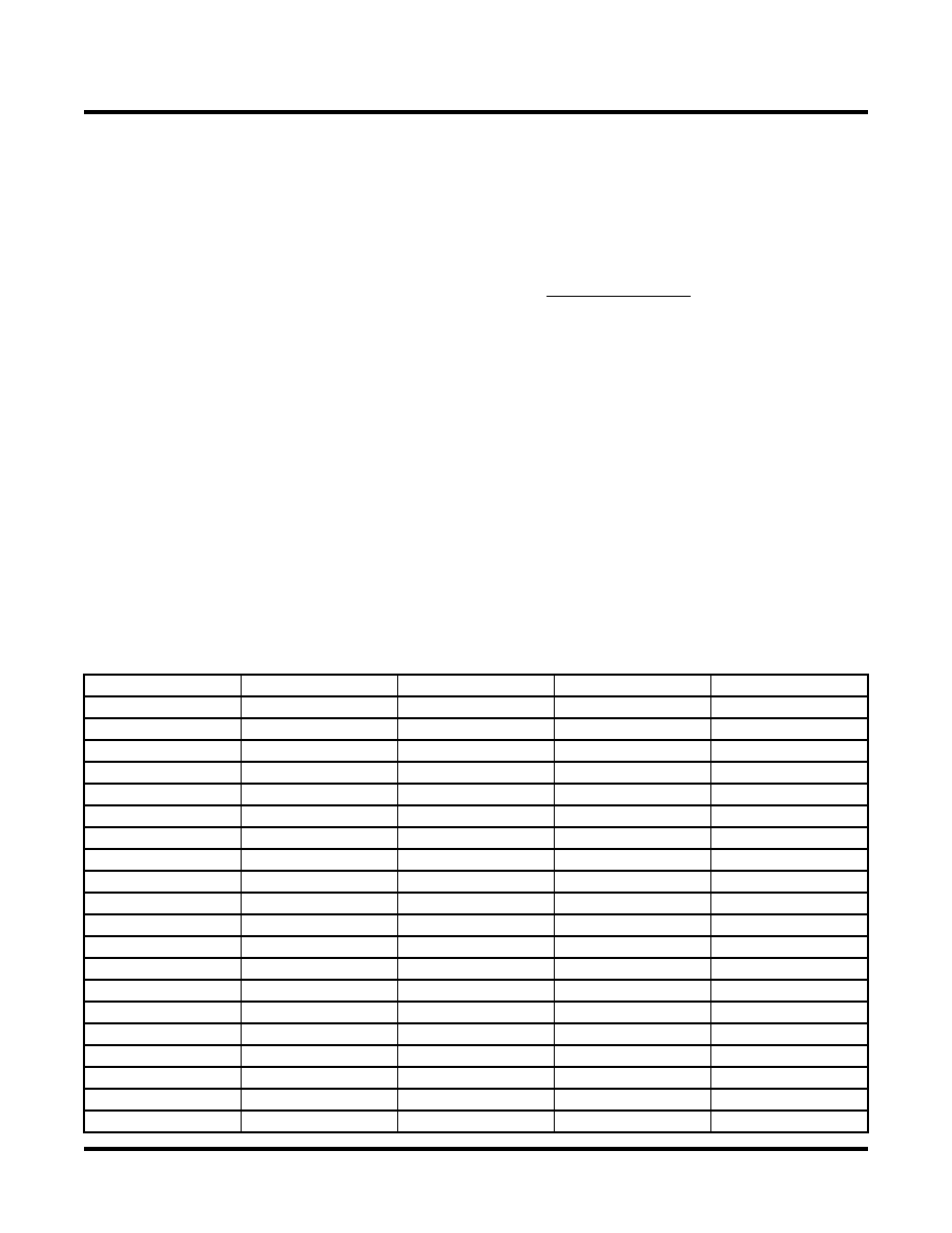
Table 13-8 provides a list of the wake up sequences supported by the LatticeXP.
Table 13-8. Wake Up Sequences Supported by LatticeXP
Sequence
Phase T0
Phase T1
Phase T2
Phase T3
1
DONE
GOE, GWDIS, GSR
2
DONE
GOE, GWDIS, GSR
3
DONE
GOE, GWDIS, GSR
4
DONE
GOE
GWDIS, GSR
5
DONE
GOE
GWDIS, GSR
6
DONE
GOE
GWDIS
GSR
7
DONE
GOE
GSR
GWDIS
8
DONE
GOE, GWDIS, GSR
9
DONE
GOE, GWDIS, GSR
10
DONE
GWDIS, GSR
GOE
11
DONE
GOE
GWDIS, GSR
12
DONE
GOE, GWDIS, GSR
13
GOE, GWDIS, GSR
DONE
14
GOE
DONE
GWDIS, GSR
15
GOE, GWDIS
DONE
GSR
16
GWDIS
DONE
GOE, GSR
17
GWDIS, GSR
DONE
GOE
18
GOE, GSR
DONE
GWDIS
19
GOE, GWDIS, GSR
DONE
20
GOE, GWDIS, GSR
DONE
相关PDF资料 |
PDF描述 |
|---|---|
| ABC49DRXS | CONN EDGECARD 98POS .100 DIP SLD |
| LFXP6C-4F256C | IC FPGA 5.8KLUTS 188I/O 256-BGA |
| LFXP6C-3FN256I | IC FPGA 5.8KLUTS 188I/O 256-BGA |
| LFXP6C-3F256I | IC FPGA 5.8KLUTS 188I/O 256-BGA |
| ABB30DHBT | CONN EDGECARD 60POS R/A .050 SLD |
相关代理商/技术参数 |
参数描述 |
|---|---|
| LFXP6E-3Q208C | 功能描述:FPGA - 现场可编程门阵列 5.8K LUTs 142 IO 1.2 V -3 Spd RoHS:否 制造商:Altera Corporation 系列:Cyclone V E 栅极数量: 逻辑块数量:943 内嵌式块RAM - EBR:1956 kbit 输入/输出端数量:128 最大工作频率:800 MHz 工作电源电压:1.1 V 最大工作温度:+ 70 C 安装风格:SMD/SMT 封装 / 箱体:FBGA-256 |
| LFXP6E-3Q208I | 功能描述:FPGA - 现场可编程门阵列 5.8K LUTs 142 IO 1.2 V -3 Spd I RoHS:否 制造商:Altera Corporation 系列:Cyclone V E 栅极数量: 逻辑块数量:943 内嵌式块RAM - EBR:1956 kbit 输入/输出端数量:128 最大工作频率:800 MHz 工作电源电压:1.1 V 最大工作温度:+ 70 C 安装风格:SMD/SMT 封装 / 箱体:FBGA-256 |
| LFXP6E-3QN208C | 功能描述:FPGA - 现场可编程门阵列 5.8K LUTs 142 IO 1.2 V -3 Spd RoHS:否 制造商:Altera Corporation 系列:Cyclone V E 栅极数量: 逻辑块数量:943 内嵌式块RAM - EBR:1956 kbit 输入/输出端数量:128 最大工作频率:800 MHz 工作电源电压:1.1 V 最大工作温度:+ 70 C 安装风格:SMD/SMT 封装 / 箱体:FBGA-256 |
| LFXP6E-3QN208I | 功能描述:FPGA - 现场可编程门阵列 5.8K LUTs 142 IO 1.2 V -3 Spd I RoHS:否 制造商:Altera Corporation 系列:Cyclone V E 栅极数量: 逻辑块数量:943 内嵌式块RAM - EBR:1956 kbit 输入/输出端数量:128 最大工作频率:800 MHz 工作电源电压:1.1 V 最大工作温度:+ 70 C 安装风格:SMD/SMT 封装 / 箱体:FBGA-256 |
| LFXP6E-3T144C | 功能描述:FPGA - 现场可编程门阵列 5.8K LUTs 100 IO 1.2 V -3 Spd RoHS:否 制造商:Altera Corporation 系列:Cyclone V E 栅极数量: 逻辑块数量:943 内嵌式块RAM - EBR:1956 kbit 输入/输出端数量:128 最大工作频率:800 MHz 工作电源电压:1.1 V 最大工作温度:+ 70 C 安装风格:SMD/SMT 封装 / 箱体:FBGA-256 |
发布紧急采购,3分钟左右您将得到回复。