- 您现在的位置:买卖IC网 > PDF目录1224 > LM5051MAEVAL/NOPB (National Semiconductor)BOARD EVAL FOR LM5051MA PDF资料下载
参数资料
| 型号: | LM5051MAEVAL/NOPB |
| 厂商: | National Semiconductor |
| 文件页数: | 13/23页 |
| 文件大小: | 0K |
| 描述: | BOARD EVAL FOR LM5051MA |
| 标准包装: | 1 |
| 主要目的: | 电源管理,O 环控制器/低压侧 |
| 嵌入式: | 否 |
| 已用 IC / 零件: | LM5051 |
| 已供物品: | 板 |
�� ���
���
���SNVS702D� –� OCTOBER� 2011� –� REVISED� MARCH� 2013�
�Several� factors� can� prevent� the� nFGD� pin� from� indicating� that� the� external� MOSFET� is� operating� normally.� If� the�
�LM5051� is� used� to� connect� parallel,� redundant� power� supplies,� one� of� the� connected� supplies� may� hold� the�
�INP/VSS� pin� voltage� close� enough� to� the� LM5051� INN� pin� voltage� that� the� V� SD(TST)� threshold� is� not� exceeded.�
�Additionally,� operating� with� a� high� output� capacitance� value� and� low� output� load� current� may� require� a� significant�
�amount� of� time� before� the� output� load� capacitance� is� discharged� to� the� point� where� the� V� SD(TST)� threshold� is�
�crossed� and� the� nFGD� pin� switches.�
�The� status� of� the� nFGD� pin� does� not� depend� on� the� status� of� the� OFF� pin.� The� status� of� the� nFGD� pin� depends�
�only� on� the� voltage� at� the� INN� pin� relative� to� the� INP/VSS� pin� being� above,� or� below,� the� V� SD(TST)� threshold�
�voltage.�
�The� nFGD� output� pin� requires� pull-up� to� an� external� voltage� source,� and� must� not� be� pulled� higher� than� 5.5V�
�above� the� INP/VSS� pin.� It� is� recommended� that� the� nFGD� pin� is� not� required� to� sink� more� than� 2mA.�
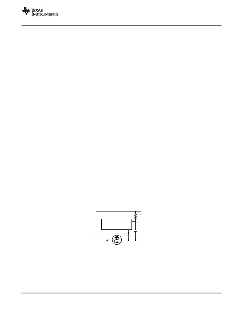
�VCC� PIN�
�The� VCC� pin� is� connected� to� the� cathode� of� the� internal� shunt� (zener)� voltage� regulator.� The� anode� of� the� shunt�
�regulator� is� connected� to� the� INP/VSS� pin.� The� VCC� pin� provides� bias� for� internal� circuitry,� as� well� as� gate� drive�
�to� the� external� MOSFET.� The� VCC� pin� should� always� be� bypassed� with� a� 0.1� μ� F� ceramic� capacitor� to� the�
�INP/VSS� pin.�
�Typically,� the� VCC� pin� is� biased� from� the� LINE� pin,� through� the� internal� 50� k� ?� series� resistor,� when� the� available�
�V� LINE� voltage� is� not� less� than� the� 36V� minimum� operating� voltage.�
�If� the� available� LINE� voltage� is� less� than� less� than� the� 36V� minimum� operating� voltage� the� VCC� pin� can� be�
�biased� through� the� use� of� an� external� resistor� to� an� appropriate� bias� supply� that� is� referenced� to� the� INP/VSS�
�pin.�
�A� minimum� VCC� pin� bias� current� of� 1� mA� is� recommended,� with� a� recommended� 10� mA� maximum.�
�A� design� example� for� calculating� the� external� resistor� where� the� VCC� pin� will� be� biased� from� an� 18V� to� 36V�
�supply� (relative� to� the� INP/VSS� pin):�
�R� BIAS� =� (V� BIAS(MIN)� -� V� Z� )� /� I� BIAS(MIN)�
�R� BIAS� =� (18V� -� 13V)� /� 1� mA�
�R� BIAS� =� 5.0� k� ?�
�(1)�
�(2)�
�(3)�
�Next,� using� the� calculated� R� BIAS� resistor� value,� verify� that� the� VCC� pin� current� will� be� no� more� than� 10mA� at� the�
�maximum� V� BIAS� voltage:�
�ICC� =� (V� BIAS(MAX)� -� 13V)� /� R� BIAS�
�ICC� =� (36V� -� 13V)� /� 5.0� k� ?�
�ICC� =� 4.6� mA�
�Since� the� calculated� 4.6� mA� is� less� than� the� 10� mA� maximum,� the� 5� k� ?� value� for� R� BIAS� is� acceptable.�
�R� BIAS�
�(4)�
�(5)�
�(6)�
�LINE�
�LM5051�
�VCC�
�INN�
�GATE� INP/VSS�
�0.1� F�
�Figure� 29.� Using� an� External� Resistor� to� Bias� the� VCC� Pin�
�Copyright� ?� 2011–2013,� Texas� Instruments� Incorporated�
�Product� Folder� Links:� LM5051�
��13�
�相关PDF资料 |
PDF描述 |
|---|---|
| LMR020-0650-CCF9-1KIT2X | KIT DEV LMR020-0650, 120V |
| LMR040-1000-CCF9-1KIT2X | KIT DEV LMR4 1000 TRUEWHITE |
| LPSJ601.ZXID | FUSEHOLDER CLASS J 60A IND 1POLE |
| LR4-1300F | POLYSWITCH PTC RESET 13A STRAP |
| LR4-170UF | POLYSWITCH PTC RESET 1.7A STRAP |
相关代理商/技术参数 |
参数描述 |
|---|---|
| LM5051MAX/NOPB | 功能描述:热插拔功率分布 Lo Side OR-ing FET Cntlr RoHS:否 制造商:Texas Instruments 产品:Controllers & Switches 电流限制: 电源电压-最大:7 V 电源电压-最小:- 0.3 V 工作温度范围: 功率耗散: 安装风格:SMD/SMT 封装 / 箱体:MSOP-8 封装:Tube |
| LM5056 | 制造商:TI 制造商全称:Texas Instruments 功能描述:High-Voltage System Power Management Device with PMBusa?¢ |
| LM5056A | 制造商:TI 制造商全称:Texas Instruments 功能描述:High-Voltage System Power Management Device with PMBusa?¢ |
| LM5056APMH/NOPB | 功能描述:PMIC 解决方案 Hi Vtg System Pwr Mgmt IC RoHS:否 制造商:Texas Instruments 安装风格:SMD/SMT 封装 / 箱体:QFN-24 封装:Reel |
| LM5056APMHE/NOPB | 功能描述:PMIC 解决方案 Hi Vtg System Pwr Mgmt IC RoHS:否 制造商:Texas Instruments 安装风格:SMD/SMT 封装 / 箱体:QFN-24 封装:Reel |
发布紧急采购,3分钟左右您将得到回复。