- 您现在的位置:买卖IC网 > PDF目录1224 > LM5051MAEVAL/NOPB (National Semiconductor)BOARD EVAL FOR LM5051MA PDF资料下载
参数资料
| 型号: | LM5051MAEVAL/NOPB |
| 厂商: | National Semiconductor |
| 文件页数: | 14/23页 |
| 文件大小: | 0K |
| 描述: | BOARD EVAL FOR LM5051MA |
| 标准包装: | 1 |
| 主要目的: | 电源管理,O 环控制器/低压侧 |
| 嵌入式: | 否 |
| 已用 IC / 零件: | LM5051 |
| 已供物品: | 板 |
�� ��
��
��SNVS702D� –� OCTOBER� 2011� –� REVISED� MARCH� 2013�
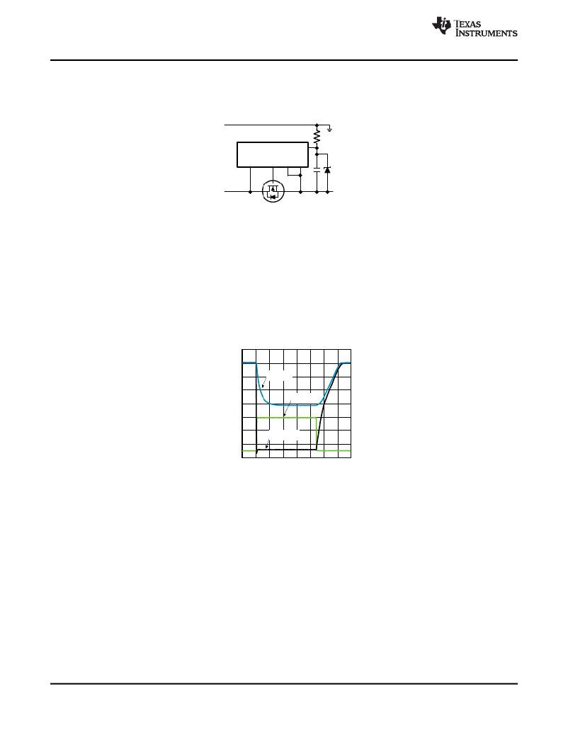
��Alternately,� an� external� bias� supply� can� be� connected� directly� to� the� VCC� pin,� as� long� as� the� applied� voltage� is�
�below� the� minimum� V� Z� breakdown� voltage� (11.9V)� and� above� the� minimum� VCC� operating� voltage� (4.50V).� In�
�this� case,� it� is� important� to� pay� close� attention� to� the� V� GS� rating� of� the� external� MOSFET� as� the� gate� drive� voltage�
�will� be� affected� by� the� lower� voltage� on� the� VCC� pin.�
�R� BIAS�
�LINE�
�LM5051�
�VCC�
�INN�
�GATE� INP/VSS�
�Figure� 30.� Using� an� External� Zener� to� Bias� the� VCC� Pin�
�In� the� case� where� the� OFF� pin� is� high� (i.e.� OR-ing� is� disabled,� and� the� Gate� is� discharged)� and� the� voltage� at� the�
�INN� pin� is� more� negative� than� the� V� SD(REV)� threshold� voltage� the� internal� current� increases,� and� the� voltage� on�
�the� VCC� pin� may� drop..� Since� the� LM5051� is� in� the� OFF� state,� this� voltage� drop� does� not� affect� any� operation.�
�However,� when� the� OFF� pin� is� taken� low� to� resume� normal� operation,� the� initial� Gate� charge� time� may� be�
�extended� slightly� if� the� capacitor� on� the� VCC� pin� has� not� had� adequate� time� to� fully� recharge� through� either� the�
�external� R� BIAS� resistor,� or� through� the� internal� 50� k� ?� resistor.�
�15�
�13�
�11�
�9�
�7�
�5�
�3�
�1�
�-1�
�VVCC�
�VGATE�
�VOFF�
�-2�
�0�
�2�
�4� 6� 8�
�10�
�12�
�14�
�TIME� (ms)�
�Figure� 31.� V� CC� and� V� GATE� vs� V� OFF� ,� V� INN� =� –100� mV�
�HIGH� SIDE� OR-ing�
�Because� the� INP� and� VSS� functions� are� internally� connected,� the� LM5051� cannot� be� configured� as� a� High-Side�
�(i.e.� Positive)� OR-ing� controller.� Please� refer� to� the� LM5050-1� and� LM5050-2� High-Side� OR-ing� controllers.�
�MOSFET� FAILURE�
�Typically,� the� INN� pin� maximum� negative� voltage� will� be� defined� by� the� body� diode� of� the� external� MOSFET.� In�
�the� even� that� the� external� MOSFET� has� a� catastrophic� failure� that� results� in� an� open� body� diode,� the� voltage�
�between� the� INP/VSS� pin� and� the� INN� pin� may� cause� current� through� the� LM5051� substrate� diode� at� the� INN�
�pin.� The� voltage� at� the� INN� pin� must� be� limited� to� a� safe� level� (� -1V)� to� prevent� damage� to� the� LM5051.� The�
�voltage� on� the� INN� pin� can� be� limited� with� the� use� of� a� Schottky� diode� and� a� current� limiting� resistor.� Note� that�
�the� power� dissipation� of� the� current� limiting� resistor� should� allow� for� any� anticipated� worst� case� condition.� See�
��14�
��Product� Folder� Links:� LM5051�
�Copyright� ?� 2011–2013,� Texas� Instruments� Incorporated�
�相关PDF资料 |
PDF描述 |
|---|---|
| LMR020-0650-CCF9-1KIT2X | KIT DEV LMR020-0650, 120V |
| LMR040-1000-CCF9-1KIT2X | KIT DEV LMR4 1000 TRUEWHITE |
| LPSJ601.ZXID | FUSEHOLDER CLASS J 60A IND 1POLE |
| LR4-1300F | POLYSWITCH PTC RESET 13A STRAP |
| LR4-170UF | POLYSWITCH PTC RESET 1.7A STRAP |
相关代理商/技术参数 |
参数描述 |
|---|---|
| LM5051MAX/NOPB | 功能描述:热插拔功率分布 Lo Side OR-ing FET Cntlr RoHS:否 制造商:Texas Instruments 产品:Controllers & Switches 电流限制: 电源电压-最大:7 V 电源电压-最小:- 0.3 V 工作温度范围: 功率耗散: 安装风格:SMD/SMT 封装 / 箱体:MSOP-8 封装:Tube |
| LM5056 | 制造商:TI 制造商全称:Texas Instruments 功能描述:High-Voltage System Power Management Device with PMBusa?¢ |
| LM5056A | 制造商:TI 制造商全称:Texas Instruments 功能描述:High-Voltage System Power Management Device with PMBusa?¢ |
| LM5056APMH/NOPB | 功能描述:PMIC 解决方案 Hi Vtg System Pwr Mgmt IC RoHS:否 制造商:Texas Instruments 安装风格:SMD/SMT 封装 / 箱体:QFN-24 封装:Reel |
| LM5056APMHE/NOPB | 功能描述:PMIC 解决方案 Hi Vtg System Pwr Mgmt IC RoHS:否 制造商:Texas Instruments 安装风格:SMD/SMT 封装 / 箱体:QFN-24 封装:Reel |
发布紧急采购,3分钟左右您将得到回复。