- 您现在的位置:买卖IC网 > Datasheet目录988 > LP5521TMEV (National Semiconductor)EVAL BOARD FOR LP5521 Datasheet资料下载
参数资料
| 型号: | LP5521TMEV |
| 厂商: | National Semiconductor |
| 文件页数: | 5/44页 |
| 文件大小: | 0K |
| 描述: | EVAL BOARD FOR LP5521 |
| 标准包装: | 1 |
| 系列: | * |
| 其它名称: | Q5109809 |
第1页第2页第3页第4页当前第5页第6页第7页第8页第9页第10页第11页第12页第13页第14页第15页第16页第17页第18页第19页第20页第21页第22页第23页第24页第25页第26页第27页第28页第29页第30页第31页第32页第33页第34页第35页第36页第37页第38页第39页第40页第41页第42页第43页第44页
�� ������
������SNVS441F� –� JANUARY� 2007� –� REVISED� FEBRUAY� 2013�
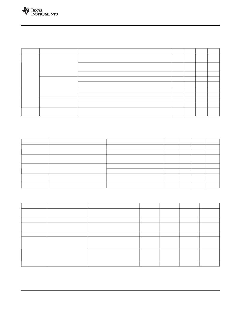
�ELECTRICAL� CHARACTERISTICS� (1)� (2)�
�Limits� in� standard� typeface� are� for� T� J� =� 25°C.� Limits� in� boldface� type� apply� over� the� operating� ambient� temperature� range� (-�
�30°C� <� T� A� <� +85°C).� Unless� otherwise� noted,� specifications� apply� to� the� LP5521� Block� Diagram� with:� 2.7V� ≤� V� DD� ≤� 5.5V,�
�C� OUT� = C� IN� =� 1� μ� F,� C� FLY1� =� C� FLY2� =� 0.47� μ� F.� (3)�
�Symbol�
�I� VDD�
�Parameter�
�Standby� supply� current�
�Condition�
�EN� =� 0� (pin),� CHIP_EN� =� 0� (bit),� external� 32� kHz� clock� running�
�Min�
�Typ�
�0.2�
�Max�
�2�
�Units�
�μ� A�
�or� not� running�
�EN� =� 1� (pin),� CHIP_EN� =� 0� (bit),� external� 32� kHz� clock� not�
�running�
�EN� =� 1� (pin),� CHIP_EN� =� 0� (bit),� external� 32� kHz� clock� running�
�1.0�
�1.4�
�μ� A�
�μ� A�
�Normal� mode� supply�
�current�
�Powersave� mode� supply�
�current�
�Charge� pump� and� LED� drivers� disabled�
�Charge� pump� in� 1x� mode,� no� load,� LED� drivers� disabled�
�Charge� pump� in� 1.5x� mode,� no� load,� LED� drivers� disabled�
�Charge� pump� in� 1x� mode,� no� load,� LED� drivers� enabled�
�External� 32� kHz� clock� running�
�Internal� oscillator� running�
�0.25�
�0.70�
�1.5�
�1.2�
�10�
�0.25�
�mA�
�mA�
�mA�
�mA�
�μ� A�
�mA�
�f� OSC�
�Internal� oscillator�
�frequency� accuracy�
�-4�
�-7�
�4�
�7�
�%�
�(1)�
�(2)�
�(3)�
�All� voltages� are� with� respect� to� the� potential� at� the� GND� pins.�
�Min� and� Max� limits� are� specified� by� design,� test,� or� statistical� analysis.�
�Low-ESR� Surface-Mount� Ceramic� Capacitors� (MLCCs)� used� in� setting� electrical� characteristics.�
�CHARGE� PUMP� ELECTRICAL� CHARACTERISTICS� (1)�
�Symbol�
�R� OUT�
�Parameter�
�Charge� pump� output� resistance�
�Gain� =� 1.5x�
�Condition�
�Min�
�Typ�
�3.5�
�Max�
�Units�
�?�
�Gain� =� 1x�
�1�
�?�
�f� SW�
�Switching� frequency�
�-7�
�1.25�
�7�
�MHz�
�%�
�I� GND�
�t� ON�
�V� OUT�
�Ground� current�
�V� OUT� turn-on� time� from� charge� pump�
�off� to� 1.5x� mode�
�Charge� pump� output� voltage�
�Gain� =� 1.5x�
�Gain� =� 1x�
�V� DD� =� 3.6V,� CHIP_EN� =� H�
�I� OUT� =� 60� mA�
�V� DD� =� 3.6V,� no� load,� Gain� =� 1.5x�
�1.2�
�0.5�
�100�
�4.55�
�mA�
�mA�
�μ� s�
�V�
�(1)�
�Input,� output,� and� fly� capacitors� should� be� of� the� type� X5R� or� X7R� low� ESR� ceramic� capacitor.�
�LED DRIVER� ELECTRICAL� CHARACTERISTICS� (R,� G,� B� OUTPUTS)�
�Symbol�
�I� LEAKAGE�
�Parameter�
�R,� G,� B� pin� leakage�
�Condition�
�Min�
�Typ�
�0.1�
�Max�
�1�
�Units�
�μA�
�current�
�I� MAX�
�Maximum� Source� Current�
�Outputs� R,� G,� B�
�25.5�
�mA�
�I� OUT�
�Accuracy� of� output� current� Output� current� set� to� 17.5� mA,� V� DD�
�=� 3.6V�
�-4�
�-5�
�4�
�5�
�%�
�I� MATCH�
�Matching� (1)�
�I� OUT� =� 17.5� mA,� V� DD� =� 3.6V�
�1�
�2�
�%�
�f� LED�
�LED� PWM� switching�
�PWM_HF� =� 1�
�frequency�
�Frequency� defined� by� internal�
�558�
�Hz�
�oscillator�
�PWM_HF� =� 0�
�Frequency� defined� by� 32� kHz� clock�
�(internal� or� external)�
�256�
�Hz�
�V� SAT�
�Saturation� voltage� (2)�
�I� OUT� set� to� 17.5� mA�
�50�
�100�
�mV�
�(1)�
�(2)�
�Matching� is� the� maximum� difference� from� the� average� of� the� three� output's� currents.�
�Saturation� voltage� is� defined� as� the� voltage� when� the� LED� current� has� dropped� 10%� from� the� value� measured� at� V� OUT� -� 1V.�
�Copyright� ?� 2007–2013,� Texas� Instruments� Incorporated�
�Product� Folder� Links:� LP5521�
��5�
�相关PDF资料 |
PDF描述 |
|---|---|
| LPS0300H1000JB | RESISTOR HEAT SINK 100 OHM 300W |
| LPS0600H4R70JB | RESISTOR HEAT SINK 4.7 OHM 600W |
| LPS0800H1000JB | RESISTOR HEAT SINK 100 OHM 800W |
| LPS1100H47R0JB | RESISTOR HEAT SINK 47 OHM 1100W |
| LR1000 | LINE CONDITIONER 1000W 4OUT |
相关代理商/技术参数 |
参数描述 |
|---|---|
| LP5521TMX | 制造商:NSC 制造商全称:National Semiconductor 功能描述:Programmable Three Channel LED Driver |
| LP5521TMX/NOPB | 功能描述:LED照明驱动器 RoHS:否 制造商:STMicroelectronics 输入电压:11.5 V to 23 V 工作频率: 最大电源电流:1.7 mA 输出电流: 最大工作温度: 安装风格:SMD/SMT 封装 / 箱体:SO-16N |
| LP5521YQ | 制造商:NSC 制造商全称:National Semiconductor 功能描述:Programmable Three Channel LED Driver |
| LP5521YQ/NOPB | 功能描述:LED照明驱动器 3 Ch Prog Led Driver LLP RoHS:否 制造商:STMicroelectronics 输入电压:11.5 V to 23 V 工作频率: 最大电源电流:1.7 mA 输出电流: 最大工作温度: 安装风格:SMD/SMT 封装 / 箱体:SO-16N |
| LP5521YQ/S7002688 | 制造商:Rochester Electronics LLC 功能描述: 制造商:Texas Instruments 功能描述: |
发布紧急采购,3分钟左右您将得到回复。