- 您现在的位置:买卖IC网 > PDF目录14461 > LT1425IS#PBF (Linear Technology)IC REG FLYBK ISOLATED .2A 16SOIC PDF资料下载
参数资料
| 型号: | LT1425IS#PBF |
| 厂商: | Linear Technology |
| 文件页数: | 16/20页 |
| 文件大小: | 0K |
| 描述: | IC REG FLYBK ISOLATED .2A 16SOIC |
| 标准包装: | 50 |
| 类型: | 回扫,隔离 |
| 输出数: | 1 |
| 输入电压: | 2.8 V ~ 20 V |
| PWM 型: | 电流模式 |
| 频率 - 开关: | 285kHz |
| 电流 - 输出: | 200mA |
| 同步整流器: | 无 |
| 工作温度: | -40°C ~ 100°C |
| 安装类型: | 表面贴装 |
| 封装/外壳: | 16-SOIC(0.154",3.90mm 宽) |
| 包装: | 管件 |
| 供应商设备封装: | 16-SOIC |
| 产品目录页面: | 1327 (CN2011-ZH PDF) |
�� �
�
�LT1425�
�APPLICATIO� N� S� I� N� FOR� M� ATIO� N�
�)� )�
�I� IN� =� 7mA� +� DC� SW�
�Average� supply� current� (including� driver� current)� is:�
�I�
�35�
�where,�
�I� SW� =� Switch� current�
�DC� =� On� switch� duty� cycle�
�Switch� power� dissipation� is� given� by:�
�P� SW� =� (I� SW� )� 2� (R� SW� )(DC)�
�R� SW� =� Output� switch� ON� resistance�
�Total� power� dissipation� of� the� die� is� the� sum� of� supply�
�current� times� supply� voltage� plus� switch� power:�
�P� D(TOTAL)� =� (I� IN� ?� V� IN� )� +� P� SW�
�FREQUENCY� COMPENSATION�
�Loop� frequency� compensation� is� performed� by� connect-�
�ing� a� capacitor� from� the� output� of� the� error� amplifier� (V� C�
�pin)� to� ground.� An� additional� series� resistor,� often�
�required� in� traditional� current� mode� switcher� controllers�
�is� usually� not� required,� and� can� even� prove� detrimental.�
�The� phase� margin� improvement� traditionally� offered� by�
�this� extra� resistor� will� usually� be� already� accomplished� by�
�the� nonzero� secondary� circuit� impedance,� which� adds� a�
�next� cycle.� This� action� naturally� holds� the� V� C� voltage� stable�
�during� the� current� comparator� sense� action� (current� mode�
�switching).�
�PCB� LAYOUT� CONSIDERATIONS�
�For� maximum� efficiency,� switch� rise� and� fall� times� are�
�made� as� short� as� practical.� To� prevent� radiation� and� high�
�frequency� resonance� problems,� proper� layout� of� the� com-�
�ponents� connected� to� the� IC� is� essential,� especially� the�
�power� paths� (primary� and� secondary).� B� field� (magnetic)�
�radiation� is� minimized� by� keeping� output� diode,� switch� pin�
�and� output� bypass� capacitor� leads� as� short� as� possible.� E�
�field� radiation� is� kept� low� by� minimizing� the� length� and�
�area� of� all� traces� connected� to� the� switch� pin.� A� ground�
�plane� should� always� be� used� under� the� switcher� circuitry�
�to� prevent� interplane� coupling.�
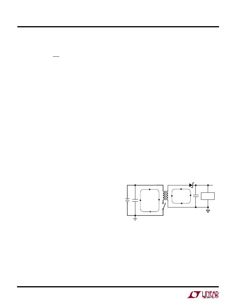
�The� high� speed� switching� current� paths� are� shown� sche-�
�matically� in� Figure� 2.� Minimum� lead� length� in� these� paths�
�are� essential� to� ensure� clean� switching� and� minimal� EMI.�
�The� path� containing� the� input� capacitor,� transformer� pri-�
�mary,� output� switch,� the� path� containing� the� transformer�
�secondary,� output� diode� and� output� capacitor� are� the� only�
�ones� containing� nanosecond� rise� and� fall� times.� Keep�
�these� paths� as� short� as� possible.�
�V� OUT�
�“zero”� to� the� loop� response.�
�In� further� contrast� to� traditional� current� mode� switchers,�
�V� IN�
�HIGH�
�FREQUENCY�
�CIRCULATING�
�?�
�?�
�HIGH�
�FREQUENCY�
�CIRCULATING�
�PATH�
�ISOLATED�
�LOAD�
�V� C� pin� ripple� is� generally� not� an� issue� with� the� LT1425.� The�
�dynamic� nature� of� the� clamped� feedback� amplifier� forms�
�an� effective� track/hold� type� response,� whereby� the� V� C�
�voltage� changes� during� the� flyback� pulse,� but� is� then�
�“held”� during� the� subsequent� “switch� ON”� portion� of� the�
�16�
�PATH�
�Figure� 2�
�F�
�1425� F02�
�相关PDF资料 |
PDF描述 |
|---|---|
| HBM24DSXN | CONN EDGECARD 48POS DIP .156 SLD |
| RBC30DRAH-S734 | CONN EDGECARD 60POS .100 R/A PCB |
| HCM24DSXH | CONN EDGECARD 48POS DIP .156 SLD |
| HBM24DSXH | CONN EDGECARD 48POS DIP .156 SLD |
| HCM24DRXN | CONN EDGECARD 48POS DIP .156 SLD |
相关代理商/技术参数 |
参数描述 |
|---|---|
| LT14-2-FP | 制造商:Thomas & Betts 功能描述:LT14-2 FOOD PROCESSINGOUTLET BOX 制造商:Thomas & Betts 功能描述:Fittings Gang Box 0.75inch Female Aluminum |
| LT1431 | 制造商:LINER 制造商全称:Linear Technology 功能描述:Synchronous Rectifier Driver for Forward Converters |
| LT1431_10 | 制造商:LINER 制造商全称:Linear Technology 功能描述:Programmable Reference |
| LT1431C | 制造商:LINER 制造商全称:Linear Technology 功能描述:Programmable Reference |
| LT1431CN8 | 功能描述:IC VREF SHUNT ADJ 8-PDIP RoHS:否 类别:集成电路 (IC) >> PMIC - 电压基准 系列:- 产品培训模块:Voltage Reference Basics 标准包装:100 系列:- 基准类型:旁路,精度 输出电压:4.096V 容差:±0.075% 温度系数:50ppm/°C 输入电压:- 通道数:1 电流 - 阴极:1µA 电流 - 静态:- 电流 - 输出:10mA 工作温度:0°C ~ 70°C 安装类型:表面贴装 封装/外壳:8-SOIC(0.154",3.90mm 宽) 供应商设备封装:8-SOIC 包装:管件 |
发布紧急采购,3分钟左右您将得到回复。