- 您现在的位置:买卖IC网 > PDF目录44982 > LT1766HGN#PBF (LINEAR TECHNOLOGY CORP) 3 A SWITCHING REGULATOR, 228 kHz SWITCHING FREQ-MAX, PDSO16 PDF资料下载
参数资料
| 型号: | LT1766HGN#PBF |
| 厂商: | LINEAR TECHNOLOGY CORP |
| 元件分类: | 稳压器 |
| 英文描述: | 3 A SWITCHING REGULATOR, 228 kHz SWITCHING FREQ-MAX, PDSO16 |
| 封装: | 0.150 INCH, LEAD FREE, PLASTIC, SSOP-16 |
| 文件页数: | 14/28页 |
| 文件大小: | 284K |
| 代理商: | LT1766HGN#PBF |
第1页第2页第3页第4页第5页第6页第7页第8页第9页第10页第11页第12页第13页当前第14页第15页第16页第17页第18页第19页第20页第21页第22页第23页第24页第25页第26页第27页第28页
21
LT1766/LT1766-5
1766fb
voltage required for full saturation of the internal power
switch. For output voltages of 5V, VC2 is approximately 5V.
During switch turn on, VC2 will fall as the boost capacitor
C2 is dicharged by the boost pin. In the previous Boost Pin
section, the value of C2 was designed for a 0.7V droop in
VC2 = VDROOP. Hence, an output voltage as low as 4V
would still allow the minimum 3.3V for the boost function
using the C2 capacitor calculated. If a target output voltage
of 12V is required, however, an excess of 8V is placed
across the boost capacitor which is not required for the
boost function but still dissipates additional power.
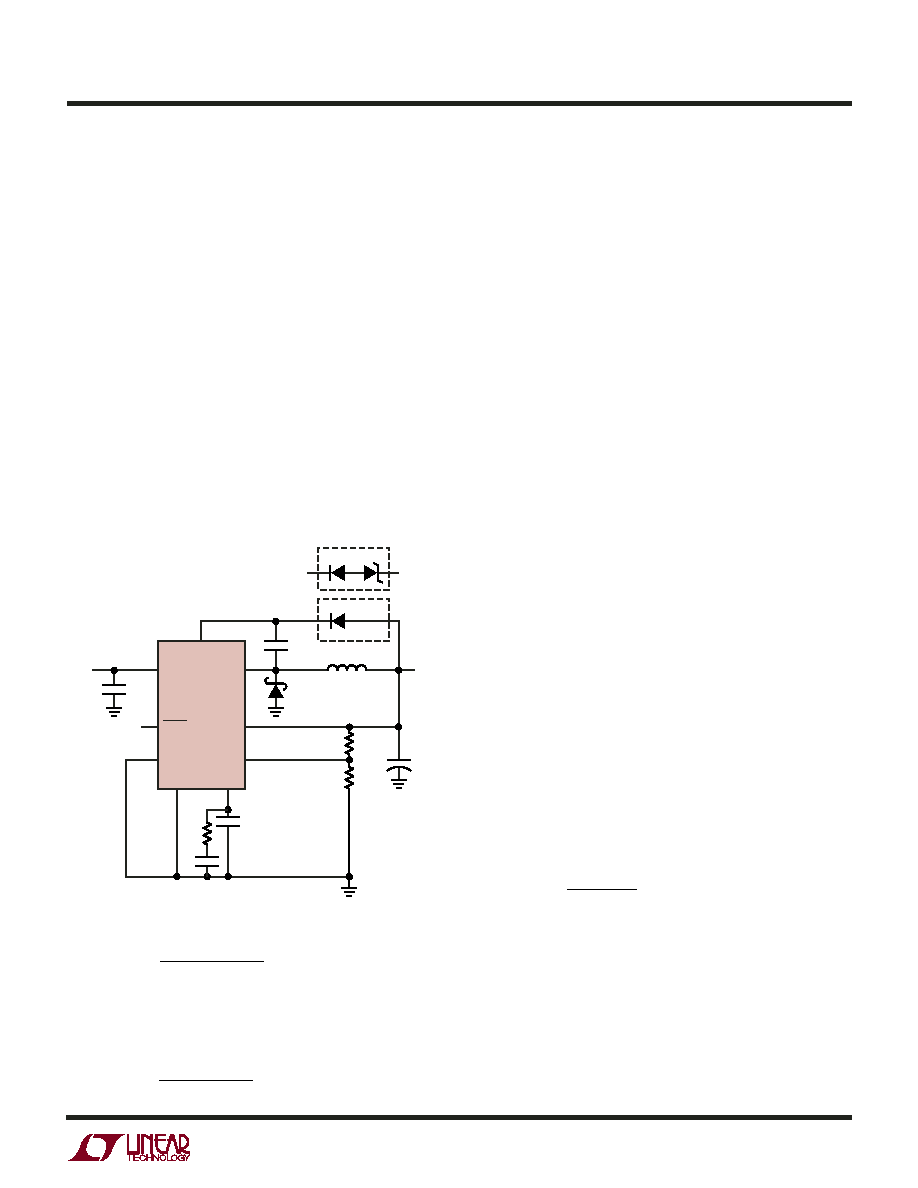
What is required is a voltage drop in the path of D2 to
achieve minimal power dissipation while still maintaining
minimum boost voltage across C2. A zener, D4, placed in
series with D2 (see Figure 9), drops voltage to C2.
Example : the BOOST pin power dissipation for a 20V input
to 12V output conversion at 1A is given by:
APPLICATIO S I FOR ATIO
WU
UU
For an FE package with thermal resistance of 45
°C/W,
ambient temperature savings would be, T(ambient) sav-
ings = 0.116W 45
°C/W = 5c. For a GN Package with
thermal resistance of 85
°C/W, ambient temperature sav-
ings would be T/(ambient) savings = 0.116 85
°C/W =
10c. The 7V zener should be sized for excess of 0.116W
operation. The tolerances of the zener should be consid-
ered to ensure minimum VC2 exceeds 3.3V + VDROOP.
Input Voltage vs Operating Frequency Considerations
The absolute maximum input supply voltage for the LT1766
is specified at 60V. This is based solely on internal semi-
conductor junction breakdown effects. Due to internal
power dissipation, the actual maximum VIN achievable in
a particular application may be less than this.
A detailed theoretical basis for estimating internal power
loss is given in the section, Thermal Considerations. Note
that AC switching loss is proportional to both operating
frequency and output current. The majority of AC switch-
ing loss is also proportional to the
square of input voltage.
For example, while the combination of VIN = 40V, VOUT =
5V at 1A and fOSC = 200kHz may be easily achievable,
simultaneously raising VIN to 60V and fOSC to 700kHz is
not possible. Nevertheless, input voltage
transients up to
60V can usually be accommodated, assuming the result-
ing increase in internal dissipation is of insufficient time
duration to raise die temperature significantly.
A second consideration is controllability. A potential limi-
tation occurs with a high step-down ratio of VIN to VOUT,
as this requires a correspondingly narrow minimum switch
on time. An approximate expression for this (assuming
continuous mode operation) is given as follows:
Min t
VV
Vf
ON
OUT
F
IN
OSC
=
+
()
where:
VIN = input voltage
VOUT = output voltage
VF = Schottky diode forward drop
fOSC = switching frequency
A potential controllability problem arises if the LT1766 is
called upon to produce an on time shorter than it is able to
produce. Feedback loop action will lower then reduce the
BOOST
VIN
D1
R1
VOUT
CF
CC
LT1766
SHDN
SYNC
SW
BIAS
FB
VC
GND
C2
C1
L1
D2
R2
1766 F09
C3
VIN
D2
D4
+
RC
PW
BOOST ==
12 1 36 12
20
02
( /
)
.
If a 7V zener D4 is placed in series with D2, then power
dissipation becomes :
PW
BOOST ==
12 1 36 5
20
0 084
( /
)
.
Figure 9. Boost Pin, Diode Selection
相关PDF资料 |
PDF描述 |
|---|---|
| LT1776IS8#TR | 1 A SWITCHING REGULATOR, 230 kHz SWITCHING FREQ-MAX, PDSO8 |
| LT1871IMS-7#PBF | SWITCHING CONTROLLER, 1000 kHz SWITCHING FREQ-MAX, PDSO10 |
| LT1871IMS-7 | SWITCHING CONTROLLER, 1000 kHz SWITCHING FREQ-MAX, PDSO10 |
| LT1871EMS-7#PBF | SWITCHING CONTROLLER, 1000 kHz SWITCHING FREQ-MAX, PDSO10 |
| LT1871EMS-7 | SWITCHING CONTROLLER, 1000 kHz SWITCHING FREQ-MAX, PDSO10 |
相关代理商/技术参数 |
参数描述 |
|---|---|
| LT1766IFE | 功能描述:IC REG BUCK ADJ 1.5A 16TSSOP RoHS:否 类别:集成电路 (IC) >> PMIC - 稳压器 - DC DC 开关稳压器 系列:- 设计资源:Design Support Tool 标准包装:1 系列:- 类型:升压(升压) 输出类型:固定 输出数:1 输出电压:3V 输入电压:0.75 V ~ 2 V PWM 型:- 频率 - 开关:- 电流 - 输出:100mA 同步整流器:是 工作温度:-40°C ~ 85°C 安装类型:表面贴装 封装/外壳:SOT-23-5 细型,TSOT-23-5 包装:剪切带 (CT) 供应商设备封装:TSOT-23-5 其它名称:AS1323-BTTT-30CT |
| LT1766IFE#PBF | 功能描述:IC REG BUCK ADJ 1.5A 16TSSOP RoHS:是 类别:集成电路 (IC) >> PMIC - 稳压器 - DC DC 开关稳压器 系列:- 产品培训模块:MIC23xxx HyperLight Load™ Regulators 标准包装:5,000 系列:HyperLight Load® 类型:降压(降压) 输出类型:固定 输出数:1 输出电压:1.8V 输入电压:2.7 V ~ 5.5 V PWM 型:混合物 频率 - 开关:4MHz 电流 - 输出:2A 同步整流器:是 工作温度:-40°C ~ 125°C 安装类型:表面贴装 封装/外壳:8-VFDFN 裸露焊盘,8-MLF? 包装:带卷 (TR) 供应商设备封装:8-MLF?(2x2) 产品目录页面:1094 (CN2011-ZH PDF) 其它名称:576-3303-2 |
| LT1766IFE#PBF | 制造商:Linear Technology 功能描述:IC STEP-DOWN REGULATOR 16-TSSOP |
| LT1766IFE#TR | 功能描述:IC REG BUCK ADJ 1.5A 16TSSOP RoHS:否 类别:集成电路 (IC) >> PMIC - 稳压器 - DC DC 开关稳压器 系列:- 设计资源:Design Support Tool 标准包装:1 系列:- 类型:升压(升压) 输出类型:固定 输出数:1 输出电压:3V 输入电压:0.75 V ~ 2 V PWM 型:- 频率 - 开关:- 电流 - 输出:100mA 同步整流器:是 工作温度:-40°C ~ 85°C 安装类型:表面贴装 封装/外壳:SOT-23-5 细型,TSOT-23-5 包装:剪切带 (CT) 供应商设备封装:TSOT-23-5 其它名称:AS1323-BTTT-30CT |
| LT1766IFE#TRPBF | 功能描述:IC REG BUCK ADJ 1.5A 16TSSOP RoHS:是 类别:集成电路 (IC) >> PMIC - 稳压器 - DC DC 开关稳压器 系列:- 设计资源:Design Support Tool 标准包装:1 系列:- 类型:升压(升压) 输出类型:固定 输出数:1 输出电压:3V 输入电压:0.75 V ~ 2 V PWM 型:- 频率 - 开关:- 电流 - 输出:100mA 同步整流器:是 工作温度:-40°C ~ 85°C 安装类型:表面贴装 封装/外壳:SOT-23-5 细型,TSOT-23-5 包装:剪切带 (CT) 供应商设备封装:TSOT-23-5 其它名称:AS1323-BTTT-30CT |
发布紧急采购,3分钟左右您将得到回复。