- 您现在的位置:买卖IC网 > PDF目录14458 > LT1941EFE#PBF (Linear Technology)IC REG MULTI CONFIG TRPL 28TSSOP PDF资料下载
参数资料
| 型号: | LT1941EFE#PBF |
| 厂商: | Linear Technology |
| 文件页数: | 13/24页 |
| 文件大小: | 0K |
| 描述: | IC REG MULTI CONFIG TRPL 28TSSOP |
| 标准包装: | 50 |
| 类型: | 降压(降压),升压(升压),反相,Sepic |
| 输出类型: | 可调式 |
| 输出数: | 3 |
| 输出电压: | 1.25 V ~ 40 V |
| 输入电压: | 3.5 V ~ 25 V |
| PWM 型: | 电流模式 |
| 频率 - 开关: | 1.1MHz |
| 电流 - 输出: | 3A |
| 同步整流器: | 无 |
| 工作温度: | -40°C ~ 85°C |
| 安装类型: | 表面贴装 |
| 封装/外壳: | 28-SOIC(0.173",4.40mm 宽)裸露焊盘 |
| 包装: | 管件 |
| 供应商设备封装: | 28-TSSOP 裸露焊盘 |
�� �
�
�LT1941�
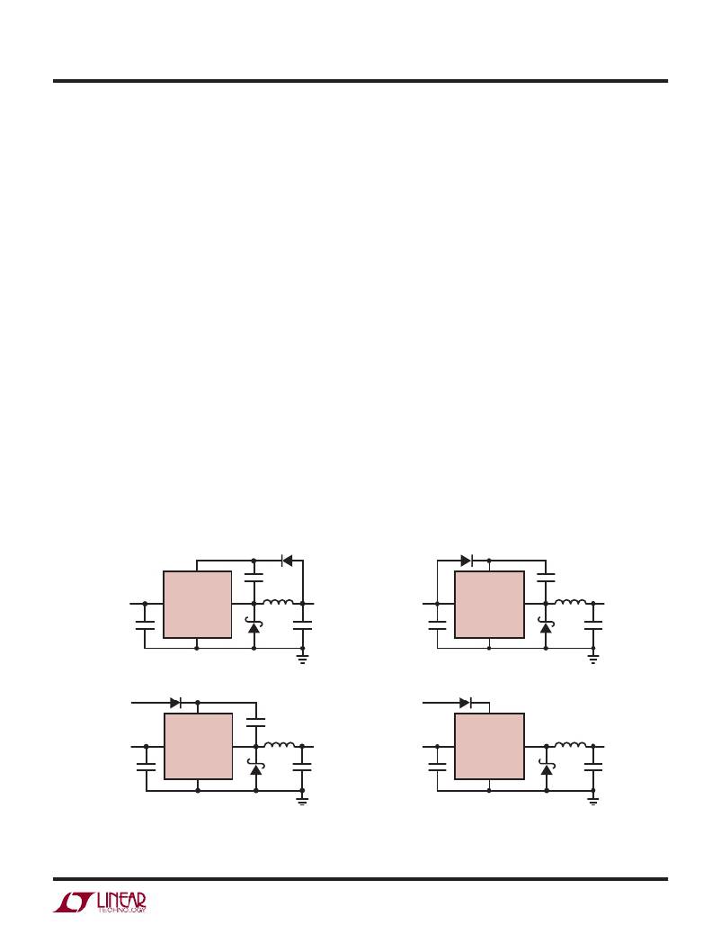
�APPLICATIONS� INFORMATION�
�Boost� Pin� Considerations�
�The� capacitor� and� diode� tied� to� the� BOOST� pin� generate�
�a� voltage� that� is� higher� than� the� input� voltage.� In� most�
�cases,� a� 0.18μF� capacitor� and� fast� switching� diode� (such�
�as� the� CMDSH-3� or� MMSD914LT1)� will� work� well.� Figure� 3�
�shows� four� ways� to� arrange� the� boost� circuit.� The� BOOST�
�pin� must� be� more� than� 2.5V� above� the� SW� pin� for� full�
�ef?ciency.� For� outputs� of� 3.3V� and� higher,� the� standard�
�circuit� (Figure� 3a)� is� best.� For� outputs� between� 2.8V� and�
�3.3V,� use� a� small� Schottky� diode� (such� as� the� BAT-54).�
�For� lower� output� voltages,� the� boost� diode� can� be� tied� to�
�the� input� (Figure� 3b).� The� circuit� in� Figure� 3a� is� more� ef�
�?cient� because� the� boost� pin� current� comes� from� a� lower�
�voltage� source.� Finally,� as� shown� in� Figure� 3c,� the� anode�
�of� the� boost� diode� can� be� tied� to� another� source� that� is�
�at� least� 3V.� For� example,� if� you� are� generating� 3.3V� and�
�1.8V� and� the� 3.3V� is� on� whenever� the� 1.8V� is� on,� the� 1.8V�
�boost� diode� can� be� connected� to� the� 3.3V� output.� In� any�
�case,� be� sure� that� the� maximum� voltage� at� the� BOOST� pin�
�is� less� than� 35V� and� the� voltage� difference� between� the�
�BOOST� and� SW� pins� is� less� than� 25V.�
�The� boost� circuit� can� also� run� directly� from� a� DC� voltage�
�that� is� higher� than� the� input� voltage� by� more� than� 2.5V� +� V� F� ,�
�as� in� Figure� 3d.� The� diode� prevents� damage� to� the� LT1941�
�D2�
�in� case� V� IN2� is� held� low� while� V� IN� is� present.� The� circuit�
�saves� several� components� (both� BOOST� pins� can� be� tied�
�to� D2).� However,� ef?ciency� may� be� lower� and� dissipation�
�in� the� LT1941� may� be� higher.� Also,� if� V� IN2� is� absent� the�
�LT1941� will� still� attempt� to� regulate� the� output,� but� will�
�do� so� with� low� ef?ciency� and� high� dissipation� because�
�the� switch� will� not� be� able� to� saturate,� dropping� 1.5V� to�
�2V� in� conduction.�
�The� minimum� operating� voltage� of� an� LT1941� application�
�is� limited� by� the� undervoltage� lockout� (3.5V)� and� by� the�
�maximum� duty� cycle.� The� boost� circuit� also� limits� the�
�minimum� input� voltage� for� proper� start-up.� If� the� input�
�voltage� ramps� slowly,� or� the� LT1941� turns� on� when� the�
�output� is� already� in� regulation,� the� boost� capacitor� may�
�not� be� fully� charged.� Because� the� boost� capacitor� charges�
�with� the� energy� stored� in� the� inductor,� the� circuit� will� rely�
�on� some� minimum� load� current� to� get� the� boost� circuit�
�running� properly.� This� minimum� load� will� depend� on� input�
�and� output� voltages,� and� on� the� arrangement� of� the� boost�
�circuit.� The� minimum� load� current� generally� goes� to� zero�
�once� the� circuit� has� started.� Even� without� an� output� load�
�current,� in� many� cases� the� discharged� output� capacitor� will�
�present� a� load� to� the� switcher� that� will� allow� it� to� start.�
�D2�
�BOOST�
�LT1941�
�C3�
�BOOST�
�LT1941�
�C3�
�V� IN�
�V� IN�
�SW�
�V� OUT�
�V� IN�
�V� IN�
�SW�
�V� OUT�
�GND�
�GND�
�V� BOOST� –� V� SW�
�MAX� V� BOOST�
�V� OUT�
�V� IN� +� V� OUT�
�(3a)�
�V� BOOST� –� V� SW�
�MAX� V� BOOST�
�V� IN�
�2V� IN�
�(3b)�
�V� IN2� >� 3V�
�D2�
�BOOST�
�LT1941�
�C3�
�V� IN2�
�>V� IN� +� 3V�
�D2�
�BOOST�
�LT1941�
�V� IN�
�V� IN�
�SW�
�V� OUT�
�V� IN�
�V� IN�
�SW�
�V� OUT�
�GND�
�GND�
�V� BOOST� –� V� SW�
�MAX� V� BOOST�
�V� IN2�
�V� IN2� +� V� IN�
�MAX� V� BOOST� –� V� SW�
�MAX� V� BOOST�
�V� IN2�
�V� IN2�
�1941� F03�
�MINIMUM� VALUE� FOR� V� IN2� =� 3V�
�(3c)�
�MINIMUM� VALUE� FOR� V� IN2� =� V� IN� +� 3V�
�(3d)�
�Figure� 3.� Generating� the� Boost� Voltage�
�1941fb�
�13�
�相关PDF资料 |
PDF描述 |
|---|---|
| LT1506CR-3.3#PBF | IC REG BUCK 3.3V 4.5A D2PAK |
| RCA35DTAN | CONN EDGECARD 70POS R/A .125 SLD |
| EBM10DTAT-S273 | CONN EDGECARD 20POS R/A .156 SLD |
| RCA35DTAH | CONN EDGECARD 70POS R/A .125 SLD |
| RCA35DTAD | CONN EDGECARD 70POS R/A .125 SLD |
相关代理商/技术参数 |
参数描述 |
|---|---|
| LT1942 | 制造商:LINER 制造商全称:Linear Technology 功能描述:Quad DCDC Converter for Triple Outputs TFT Supply Plus LED Driver |
| LT1942EUF | 制造商:Linear Technology 功能描述:Conv DC-DC Quad Inv/Step Up 2.6V to 16V 24-Pin QFN EP |
| LT1942EUF#PBF | 功能描述:IC REG SW QUAD TFT LCD 24-QFN RoHS:是 类别:集成电路 (IC) >> PMIC - 稳压器 - 专用型 系列:- 标准包装:43 系列:- 应用:控制器,Intel VR11 输入电压:5 V ~ 12 V 输出数:1 输出电压:0.5 V ~ 1.6 V 工作温度:-40°C ~ 85°C 安装类型:表面贴装 封装/外壳:48-VFQFN 裸露焊盘 供应商设备封装:48-QFN(7x7) 包装:管件 |
| LT1942EUF#TRPBF | 功能描述:IC REG SW QUAD TFT LCD 24-QFN RoHS:是 类别:集成电路 (IC) >> PMIC - 稳压器 - 专用型 系列:- 标准包装:43 系列:- 应用:控制器,Intel VR11 输入电压:5 V ~ 12 V 输出数:1 输出电压:0.5 V ~ 1.6 V 工作温度:-40°C ~ 85°C 安装类型:表面贴装 封装/外壳:48-VFQFN 裸露焊盘 供应商设备封装:48-QFN(7x7) 包装:管件 |
| LT1942EUFPBF | 制造商:Linear Technology 功能描述:Conv DC-DC Quad Inv/Step-Up 16V QFN24EP |
发布紧急采购,3分钟左右您将得到回复。