参数资料
| 型号: | LT3431IFE#TRPBF |
| 厂商: | Linear Technology |
| 文件页数: | 18/28页 |
| 文件大小: | 0K |
| 描述: | IC REG BUCK ADJ 3A 16TSSOP |
| 标准包装: | 2,500 |
| 类型: | 降压(降压) |
| 输出类型: | 可调式 |
| 输出数: | 1 |
| 输出电压: | 1.2 V ~ 48 V |
| 输入电压: | 5.5 V ~ 60 V |
| PWM 型: | 电流模式 |
| 频率 - 开关: | 500kHz |
| 电流 - 输出: | 3A |
| 同步整流器: | 无 |
| 工作温度: | -40°C ~ 125°C |
| 安装类型: | 表面贴装 |
| 封装/外壳: | 16-TSSOP(0.173",4.40mm)裸露焊盘 |
| 包装: | 带卷 (TR) |
| 供应商设备封装: | 16-TSSOP-EP |
第1页第2页第3页第4页第5页第6页第7页第8页第9页第10页第11页第12页第13页第14页第15页第16页第17页当前第18页第19页第20页第21页第22页第23页第24页第25页第26页第27页第28页
�� �
�
�LT3431�
�APPLICATIO� S� I� FOR� ATIO�
�The� V� C� and� FB� components� should� be� kept� as� far� away� as�
�possible� from� the� switch� and� boost� nodes.� The� LT3431�
�pinout� has� been� designed� to� aid� in� this.� The� ground� for�
�these� components� should� be� separated� from� the� switch�
�current� path.� Failure� to� do� so� will� result� in� poor� stability� or�
�subharmonic� like� oscillation.�
�Board� layout� also� has� a� significant� effect� on� thermal�
�resistance.� Pins� 1,� 8,� 9� and� 16,� GND,� are� a� continuous�
�copper� plate� that� runs� under� the� LT3431� die.� This� is� an�
�exposed� pad� and� is� the� best� thermal� path� for� heat� out� of� the�
�package.� Soldering� the� exposed� pad� to� the� copper� ground�
�plane� under� the� device� will� reduce� die� temperature� and�
�increase� the� power� capability� of� the� LT3431.� Adding�
�multiple� solder� filled� feedthroughs� under� and� around� the�
�four� corner� pins� to� the� ground� plane� will� also� help.� Similar�
�treatment� to� the� catch� diode� and� coil� terminations� will�
�reduce� any� additional� heating� effects.�
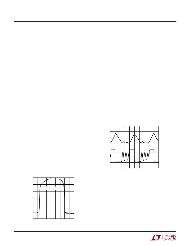
�PARASITIC� RESONANCE�
�Resonance� or� “ringing”� may� sometimes� be� seen� on� the�
�switch� node� (see� Figure� 7).� Very� high� frequency� ringing�
�following� switch� rise� time� is� caused� by� switch/diode/input�
�absolute� max� switch� voltage.� The� path� around� switch,�
�catch� diode� and� input� capacitor� must� be� kept� as� short� as�
�possible� to� ensure� reliable� operation.� When� looking� at� this,�
�a� >100MHz� oscilloscope� must� be� used,� and� waveforms�
�should� be� observed� on� the� leads� of� the� package.� This�
�switch� off� spike� will� also� cause� the� SW� node� to� go� below�
�ground.� The� LT3431� has� special� circuitry� inside� which�
�mitigates� this� problem,� but� negative� voltages� over� 0.8V�
�lasting� longer� than� 10ns� should� be� avoided.� Note� that�
�100MHz� oscilloscopes� are� barely� fast� enough� to� see� the�
�details� of� the� falling� edge� overshoot� in� Figure� 7.�
�A� second,� much� lower� frequency� ringing� is� seen� during�
�switch� off� time� if� load� current� is� low� enough� to� allow� the�
�inductor� current� to� fall� to� zero� during� part� of� the� switch� off�
�time� (see� Figure� 8).� Switch� and� diode� capacitance� reso-�
�nate� with� the� inductor� to� form� damped� ringing� at� 1MHz� to�
�10MHz.� This� ringing� is� not� harmful� to� the� regulator� and� it�
�has� not� been� shown� to� contribute� significantly� to� EMI.� Any�
�attempt� to� damp� it� with� a� resistive� snubber� will� degrade�
�efficiency.�
�capacitor� lead� inductance� and� diode� capacitance.� Schot-�
�tky� diodes� have� very� high� “Q”� junction� capacitance� that�
�can� ring� for� many� cycles� when� excited� at� high� frequency.�
�If� total� lead� length� for� the� input� capacitor,� diode� and�
�switch� path� is� 1� inch,� the� inductance� will� be� approximately�
�25nH.� At� switch� off,� this� will� produce� a� spike� across� the�
�NPN� output� device� in� addition� to� the� input� voltage.� At�
�higher� currents� this� spike� can� be� in� the� order� of� 10V� to� 20V�
�0.2A/DIV�
�5V/DIV�
�INDUCTOR�
�CURRENT� AT�
�I� OUT� =� 0.1A�
�SWITCH� NODE�
�VOLTAGE�
�or� higher� with� a� poor� layout,� potentially� exceeding� the�
�V� IN� =� 12V�
�V� OUT� =� 5V�
�L� =� 10� μ� H�
�500ns/DIV�
�3431� F08�
�Figure� 8.� Discontinuous� Mode� Ringing�
�2V/DIV�
�SW� RISE�
�SW� FALL�
�THERMAL� CALCULATIONS�
�Power� dissipation� in� the� LT3431� chip� comes� from� four�
�sources:� switch� DC� loss,� switch� AC� loss,� boost� circuit�
�current,� and� input� quiescent� current.� The� following� formu-�
�las� show� how� to� calculate� each� of� these� losses.� These�
�formulas� assume� continuous� mode� operation,� so� they�
�should� not� be� used� for� calculating� efficiency� at� light� load�
�50ns/DIV�
�3431� F07�
�currents.�
�Figure� 7.� Switch� Node� Resonance�
�sn3431� 3431fs�
�18�
�相关PDF资料 |
PDF描述 |
|---|---|
| LT3433IFE#TRPBF | IC REG BUCK BST ADJ 0.5A 16TSSOP |
| LT3434IFE#TRPBF | IC REG BUCK ADJ 3A 16TSSOP |
| LT3435IFE#TRPBF | IC REG BUCK ADJ 3A 16TSSOP |
| LT3436EFE#TRPBF | IC REG BOOST ADJ 3A 16TSSOP |
| LT3437EDD#PBF | IC REG BUCK ADJ 0.5A 10DFN |
相关代理商/技术参数 |
参数描述 |
|---|---|
| LT3433 | 制造商:LINER 制造商全称:Linear Technology 功能描述:High Voltage Step-Up/Step-Down DC/DC Converter |
| LT3433_1 | 制造商:LINER 制造商全称:Linear Technology 功能描述:High Voltage Step-Up/Step-Down DC/DC Converter |
| LT3433EFE | 功能描述:IC REG BUCK BST ADJ 0.5A 16TSSOP RoHS:否 类别:集成电路 (IC) >> PMIC - 稳压器 - DC DC 开关稳压器 系列:- 标准包装:2,500 系列:- 类型:降压(降压) 输出类型:固定 输出数:1 输出电压:1.2V,1.5V,1.8V,2.5V 输入电压:2.7 V ~ 20 V PWM 型:- 频率 - 开关:- 电流 - 输出:50mA 同步整流器:是 工作温度:-40°C ~ 125°C 安装类型:表面贴装 封装/外壳:10-TFSOP,10-MSOP(0.118",3.00mm 宽)裸露焊盘 包装:带卷 (TR) 供应商设备封装:10-MSOP 裸露焊盘 |
| LT3433EFE#PBF | 功能描述:IC REG BUCK BST ADJ 0.5A 16TSSOP RoHS:是 类别:集成电路 (IC) >> PMIC - 稳压器 - DC DC 开关稳压器 系列:- 标准包装:250 系列:- 类型:降压(降压) 输出类型:固定 输出数:1 输出电压:1.2V 输入电压:2.05 V ~ 6 V PWM 型:电压模式 频率 - 开关:2MHz 电流 - 输出:500mA 同步整流器:是 工作温度:-40°C ~ 85°C 安装类型:表面贴装 封装/外壳:6-UFDFN 包装:带卷 (TR) 供应商设备封装:6-SON(1.45x1) 产品目录页面:1032 (CN2011-ZH PDF) 其它名称:296-25628-2 |
| LT3433EFE#TR | 功能描述:IC REG BUCK BST ADJ 0.5A 16TSSOP RoHS:否 类别:集成电路 (IC) >> PMIC - 稳压器 - DC DC 开关稳压器 系列:- 标准包装:2,500 系列:- 类型:降压(降压) 输出类型:固定 输出数:1 输出电压:1.2V,1.5V,1.8V,2.5V 输入电压:2.7 V ~ 20 V PWM 型:- 频率 - 开关:- 电流 - 输出:50mA 同步整流器:是 工作温度:-40°C ~ 125°C 安装类型:表面贴装 封装/外壳:10-TFSOP,10-MSOP(0.118",3.00mm 宽)裸露焊盘 包装:带卷 (TR) 供应商设备封装:10-MSOP 裸露焊盘 |
发布紧急采购,3分钟左右您将得到回复。