参数资料
| 型号: | LT3431IFE#TRPBF |
| 厂商: | Linear Technology |
| 文件页数: | 23/28页 |
| 文件大小: | 0K |
| 描述: | IC REG BUCK ADJ 3A 16TSSOP |
| 标准包装: | 2,500 |
| 类型: | 降压(降压) |
| 输出类型: | 可调式 |
| 输出数: | 1 |
| 输出电压: | 1.2 V ~ 48 V |
| 输入电压: | 5.5 V ~ 60 V |
| PWM 型: | 电流模式 |
| 频率 - 开关: | 500kHz |
| 电流 - 输出: | 3A |
| 同步整流器: | 无 |
| 工作温度: | -40°C ~ 125°C |
| 安装类型: | 表面贴装 |
| 封装/外壳: | 16-TSSOP(0.173",4.40mm)裸露焊盘 |
| 包装: | 带卷 (TR) |
| 供应商设备封装: | 16-TSSOP-EP |
第1页第2页第3页第4页第5页第6页第7页第8页第9页第10页第11页第12页第13页第14页第15页第16页第17页第18页第19页第20页第21页第22页当前第23页第24页第25页第26页第27页第28页
�� �
�
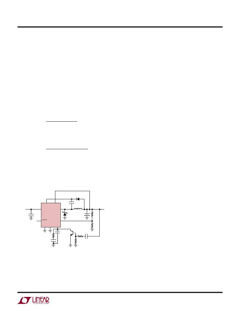
�LT3431�
�APPLICATIO� S� I� FOR� ATIO�
�BUCK� CONVERTER� WITH� ADJUSTABLE� SOFT-START�
�Large� capacitive� loads� or� high� input� voltages� can� cause�
�high� input� currents� at� start-up.� Figure� 13� shows� a� circuit�
�that� limits� the� dv/dt� of� the� output� at� start-up,� controlling�
�the� capacitor� charge� rate.� The� buck� converter� is� a� typical�
�configuration� with� the� addition� of� R3,� R4,� C� SS� and� Q1.�
�As� the� output� starts� to� rise,� Q1� turns� on,� regulating� switch�
�current� via� the� V� C� pin� to� maintain� a� constant� dv/dt� at� the�
�output.� Output� rise� time� is� controlled� by� the� current�
�through� C� SS� defined� by� R4� and� Q1’s� V� BE� .� Once� the� output�
�is� in� regulation,� Q1� turns� off� and� the� circuit� operates�
�normally.� R3� is� transient� protection� for� the� base� of� Q1.�
�Dual� Polarity� Output� Converter�
�The� circuit� in� Figure� 14a� generates� both� positive� and�
�negative� 5V� outputs� with� all� components� under� 3mm�
�height.� The� topology� for� the� 5V� output� is� a� standard� buck�
�converter.� The� –5V� output� uses� a� second� inductor� L2,�
�diode� D3,� and� output� capacitor� C6.� The� capacitor� C4�
�couples� energy� to� L2� and� ensures� equal� voltages� across�
�L2� and� L1� during� steady� state.� Instead� of� using� a� trans-�
�former� for� L1� and� L2,� uncoupled� inductors� were� used�
�because� they� require� less� height� than� a� single� transformer,�
�can� be� placed� separately� in� the� circuit� layout� for� optimized�
�space� savings� and� reduce� overall� cost.� This� is� true� even�
�Rise� Time� =�
�(� R� 4� )(� C� SS� )(� V� OUT� )�
�V� BE�
�when� the� uncoupled� inductors� are� sized� (twice� the� value� of�
�inductance� of� the� transformer)� in� order� to� keep� ripple�
�current� comparable� to� the� transformer� solution.� If� a� single�
�transformer� becomes� available� to� provide� a� better� height�
�(� )(� )� (� )� 5� =� 5� ms�
�47� ?� 10� 15� ?� 10�
�Using the values shown in Figure 10,�
�3� –� 9�
�Rise� Time� =�
�0� .� 7�
�The� ramp� is� linear� and� rise� times� in� the� order� of� 100ms� are�
�possible.� Since� the� circuit� is� voltage� controlled,� the� ramp�
�rate� is� unaffected� by� load� characteristics� and� maximum�
�output� current� is� unchanged.� Variants� of� this� circuit� can� be�
�used� for� sequencing� multiple� regulator� outputs.�
�D2�
�MMSD914TI�
�/cost� solution,� refer� to� the� Dual� Output� SEPIC� circuit�
�description� in� Design� Note� 100� for� correct� transformer�
�connection.�
�During� switch� on-time,� in� steady� state,� the� voltage� across�
�both� L1� and� L2� is� positive� and� equal� ;� with� energy� (and�
�current)� ramping� up� in� each� inductor.� The� current� in� L2� is�
�provided� by� the� coupling� capacitor� C4.� During� switch� off-�
�time,� current� ramps� downward� in� each� inductor.� The�
�current� in� L2� and� C4� flows� via� the� catch� diode� D3,� charging�
�the� negative� output� capacitor� C6.� If� the� negative� output� is�
�not� loaded� enough� it� can� go� severely� unregulated� (become�
�more� negative).� Figure� 14b� shows� the� maximum� allow-�
�0.22� μ� F�
�C1�
�10V�
�INPUT�
�12V�
�C3�
�4.7� μ� F�
�25V�
�CER�
�BOOST� BIAS�
�LT3431�
�SHDN� FB�
�V� IN� SW�
�C2�
�L1�
�15� μ� H�
�D1�
�30BQ060� 100� μ� F�
�OR� B250A�
�+�
�R1�
�15.4k�
�OUTPUT�
�5V�
�2A�
�able� –5V� output� load� current� (vs� load� current� on� the� 5V�
�output)� that� will� maintain� the� –5V� output� within� 3%�
�tolerance.� Figure� 14c� shows� the� –5V� output� voltage� regu-�
�lation� versus� its� own� load� current� when� plotted� for� three�
�SYNC� GND�
�V� C�
�R2�
�4.99k�
�separate� load� currents� on� the� 5V� output.� The� efficiency� of�
�R� C�
�3.3k�
�C� C�
�0.022� μ� F�
�C� F�
�220pF� Q1�
�R3�
�2k�
�R4�
�47k�
�C� SS�
�15nF�
�3431� F13�
�the� dual� polarity� output� converter� circuit� shown� in� Figure�
�14a� is� given� in� Figure� 14d.�
�L1:� CDRH104R-220M�
�Figure� 13.� Buck� Converter� with� Adjustable� Soft-Start�
�sn3431� 3431fs�
�23�
�相关PDF资料 |
PDF描述 |
|---|---|
| LT3433IFE#TRPBF | IC REG BUCK BST ADJ 0.5A 16TSSOP |
| LT3434IFE#TRPBF | IC REG BUCK ADJ 3A 16TSSOP |
| LT3435IFE#TRPBF | IC REG BUCK ADJ 3A 16TSSOP |
| LT3436EFE#TRPBF | IC REG BOOST ADJ 3A 16TSSOP |
| LT3437EDD#PBF | IC REG BUCK ADJ 0.5A 10DFN |
相关代理商/技术参数 |
参数描述 |
|---|---|
| LT3433 | 制造商:LINER 制造商全称:Linear Technology 功能描述:High Voltage Step-Up/Step-Down DC/DC Converter |
| LT3433_1 | 制造商:LINER 制造商全称:Linear Technology 功能描述:High Voltage Step-Up/Step-Down DC/DC Converter |
| LT3433EFE | 功能描述:IC REG BUCK BST ADJ 0.5A 16TSSOP RoHS:否 类别:集成电路 (IC) >> PMIC - 稳压器 - DC DC 开关稳压器 系列:- 标准包装:2,500 系列:- 类型:降压(降压) 输出类型:固定 输出数:1 输出电压:1.2V,1.5V,1.8V,2.5V 输入电压:2.7 V ~ 20 V PWM 型:- 频率 - 开关:- 电流 - 输出:50mA 同步整流器:是 工作温度:-40°C ~ 125°C 安装类型:表面贴装 封装/外壳:10-TFSOP,10-MSOP(0.118",3.00mm 宽)裸露焊盘 包装:带卷 (TR) 供应商设备封装:10-MSOP 裸露焊盘 |
| LT3433EFE#PBF | 功能描述:IC REG BUCK BST ADJ 0.5A 16TSSOP RoHS:是 类别:集成电路 (IC) >> PMIC - 稳压器 - DC DC 开关稳压器 系列:- 标准包装:250 系列:- 类型:降压(降压) 输出类型:固定 输出数:1 输出电压:1.2V 输入电压:2.05 V ~ 6 V PWM 型:电压模式 频率 - 开关:2MHz 电流 - 输出:500mA 同步整流器:是 工作温度:-40°C ~ 85°C 安装类型:表面贴装 封装/外壳:6-UFDFN 包装:带卷 (TR) 供应商设备封装:6-SON(1.45x1) 产品目录页面:1032 (CN2011-ZH PDF) 其它名称:296-25628-2 |
| LT3433EFE#TR | 功能描述:IC REG BUCK BST ADJ 0.5A 16TSSOP RoHS:否 类别:集成电路 (IC) >> PMIC - 稳压器 - DC DC 开关稳压器 系列:- 标准包装:2,500 系列:- 类型:降压(降压) 输出类型:固定 输出数:1 输出电压:1.2V,1.5V,1.8V,2.5V 输入电压:2.7 V ~ 20 V PWM 型:- 频率 - 开关:- 电流 - 输出:50mA 同步整流器:是 工作温度:-40°C ~ 125°C 安装类型:表面贴装 封装/外壳:10-TFSOP,10-MSOP(0.118",3.00mm 宽)裸露焊盘 包装:带卷 (TR) 供应商设备封装:10-MSOP 裸露焊盘 |
发布紧急采购,3分钟左右您将得到回复。