- 您现在的位置:买卖IC网 > PDF目录14838 > LT3487EDD#PBF (Linear Technology)IC REG BOOST INV ADJ 10DFN PDF资料下载
参数资料
| 型号: | LT3487EDD#PBF |
| 厂商: | Linear Technology |
| 文件页数: | 11/16页 |
| 文件大小: | 0K |
| 描述: | IC REG BOOST INV ADJ 10DFN |
| 标准包装: | 121 |
| 类型: | 升压(升压),反相 |
| 输出类型: | 可调式 |
| 输出数: | 1 |
| 输出电压: | 1.23 V ~ 28 V |
| 输入电压: | 2.3 V ~ 16 V |
| PWM 型: | 电流模式 |
| 频率 - 开关: | 2MHz |
| 同步整流器: | 无 |
| 工作温度: | -40°C ~ 85°C |
| 安装类型: | 表面贴装 |
| 封装/外壳: | 10-WFDFN 裸露焊盘 |
| 包装: | 管件 |
| 供应商设备封装: | 10-DFN(3x3) |
| 产品目录页面: | 1331 (CN2011-ZH PDF) |
�� �
�
�LT3487�
�APPLICATIO� S� I� FOR� ATIO�
�Choosing� a� Feedback� Node�
�The� positive� channel� feedback� resistor,� R1,� may� be� con-�
�nected� to� the� V� POS� pin� or� to� the� CAP� pin� (see� Figure� 5).�
�Regulating� the� V� POS� pin� eliminates� the� output� offset� result-�
�ing� from� the� voltage� drop� across� the� output� disconnect.�
�However,� in� the� case� of� a� short-circuit� fault� at� the� V� POS�
�pin,� the� LT3487� will� switch� continuously� because� the� FBP�
�pin� is� low.� While� operating� in� this� open-loop� condition,� the�
�rising� voltage� at� the� CAP� pin� is� limited� only� by� the� current�
�limit� of� the� output� disconnect.� Given� worst-case� parameters�
�this� voltage� may� reach� 18V� in� a� Li-Ion� application.� Care�
�must� be� taken� in� high� V� IN� applications� when� regulating�
�from� the� V� POS� pin.� When� the� short-circuit� is� removed,� the�
�the� capacitor� voltages� fall� back� into� regulation.� While� this�
�is� harmless� to� the� LT3487,� this� should� be� considered� in�
�the� context� of� the� external� circuitry� if� short-circuit� events�
�are� expected.� Regulating� the� CAP� pin� ensures� that� the�
�voltage� on� the� V� POS� pin� never� exceeds� the� set� output� volt-�
�age� after� a� short-circuit� event.� However,� this� setup� does�
�not� compensate� for� the� voltage� drop� across� the� output�
�disconnect,� resulting� in� an� output� voltage� that� is� slightly�
�lower� than� the� voltage� set� by� the� feedback� resistor.� This�
�voltage� drop� (V� DISC� )� can� be� accounted� for� when� using�
�the� CAP� pin� as� the� feedback� node� by� setting� the� output�
�voltage� according� to� the� following� formula� (using� V� DISC�
�from� Figure� 4):�
�V� POS� pin� will� bounce� up� to� the� voltage� on� the� CAP� pin,�
�potentially� exceeding� the� programmed� output� voltage� until�
�R� 1� =�
�V� POS� +� V� DISC� – 1 .23�
�25� μA�
�300�
�250�
�200�
�150�
�100�
�50�
�V� BAT�
�The� V� BAT� pin� is� a� new� innovation� in� the� LT3487� that� allows�
�output� disconnect� operation� in� a� wide� range� of� applica-�
�tions.� The� V� BAT� pin� allows� the� part� to� stay� on� until� CAP� is�
�less� than� 1.2V� above� V� BAT� .� This� ensures� that� the� positive�
�bias� doesn’t� fall� before� the� negative� bias� discharges.� In�
�some� applications� it� may� be� useful� to� power� the� inductors�
�from� a� different� source� than� V� IN� .� In� this� case,� connect�
�0�
�0�
�20� 40� 60� 80�
�DISCONNECT� CURRENT� (mA)�
�100�
�2400� G31�
�V� BAT� to� the� source� powering� the� inductors� to� allow� proper�
�operation� of� the� disconnect.� For� example,� in� an� automotive�
�system� there� may� already� be� a� buck� regulator� producing�
�3.3V� from� a� 12V� battery.� The� LT3487� enables� the� user�
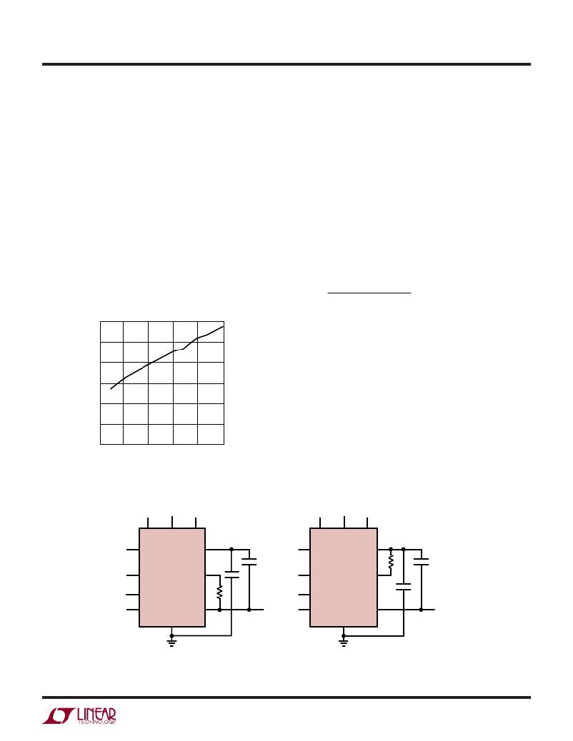
�Figure� 4.� V� CE� vs� I� of� Output� Disconnect�
�to� power� V� IN� from� the� 3.3V� rail,� but� power� the� V� BAT� pin�
�SWN�
�V� IN�
�V� BAT�
�SWP�
�CAP�
�SWN�
�V� IN�
�V� BAT�
�SWP�
�CAP�
�LT3487�
�LT3487�
�DN�
�FBN�
�FBP�
�DN�
�FBN�
�FBP�
�RUN/SS�
�V� POS�
�V� POS�
�RUN/SS�
�V� POS�
�V� POS�
�GND�
�GND�
�3487� F05�
�Figure� 5.� Feedback� Connection� Using� the� V� POS� and� CAP� Pins�
�3487f�
�11�
�相关PDF资料 |
PDF描述 |
|---|---|
| MAX6463XR43+T | IC VOLT DETECTOR LP SC70-3 |
| ADM660ARZ | IC REG MULTI CONFIG ADJ 8SOIC |
| MAX6463XR35+T | IC VOLT DETECTOR LP SC70-3 |
| PM2120-121K | INDUCTOR TOROID 120UH 10% SMD |
| LTC3419IDD#PBF | IC REG BUCK SYNC ADJ .6A DL 8DFN |
相关代理商/技术参数 |
参数描述 |
|---|---|
| LT3489 | 制造商:LINER 制造商全称:Linear Technology 功能描述:2MHz Boost DC/DC Converter with 2.5A Switch and Soft-Start |
| LT3489EMS8E | 制造商:LINER 制造商全称:Linear Technology 功能描述:2MHz Boost DC/DC Converter with 2.5A Switch and Soft-Start |
| LT3489EMS8E#PBF | 功能描述:IC REG BOOST ADJ 2.5A 8MSOP RoHS:是 类别:集成电路 (IC) >> PMIC - 稳压器 - DC DC 开关稳压器 系列:- 标准包装:250 系列:- 类型:降压(降压) 输出类型:固定 输出数:1 输出电压:1.2V 输入电压:2.05 V ~ 6 V PWM 型:电压模式 频率 - 开关:2MHz 电流 - 输出:500mA 同步整流器:是 工作温度:-40°C ~ 85°C 安装类型:表面贴装 封装/外壳:6-UFDFN 包装:带卷 (TR) 供应商设备封装:6-SON(1.45x1) 产品目录页面:1032 (CN2011-ZH PDF) 其它名称:296-25628-2 |
| LT3489EMS8E#PBF | 制造商:Linear Technology 功能描述:DC-DC CONVERTER BOOST 2MHZ 制造商:Linear Technology 功能描述:DC-DC CONVERTER, BOOST, 2MHZ, MSOP-8 |
| LT3489EMS8E#TR | 制造商:Linear Technology 功能描述:SP-SWREG/Monolithic, 2.5A, 2MHz Step-Up Regulator in MS8E |
发布紧急采购,3分钟左右您将得到回复。