- 您现在的位置:买卖IC网 > PDF目录14826 > LT3581EMSE#PBF (Linear Technology)IC REG MULTI CONFIG ADJ 16MSOP PDF资料下载
参数资料
| 型号: | LT3581EMSE#PBF |
| 厂商: | Linear Technology |
| 文件页数: | 16/36页 |
| 文件大小: | 0K |
| 描述: | IC REG MULTI CONFIG ADJ 16MSOP |
| 标准包装: | 37 |
| 类型: | 升压(升压),反相,回扫,Sepic |
| 输出类型: | 可调式 |
| 输出数: | 1 |
| 输出电压: | 1.22 V ~ 42 V |
| 输入电压: | 2.5 V ~ 22 V |
| PWM 型: | 电流模式 |
| 频率 - 开关: | 200kHz ~ 2.5MHz |
| 电流 - 输出: | 3.3A |
| 同步整流器: | 无 |
| 工作温度: | -40°C ~ 125°C |
| 安装类型: | 表面贴装 |
| 封装/外壳: | 16-TFSOP(0.118",3.00mm 宽)裸露焊盘 |
| 包装: | 管件 |
| 供应商设备封装: | 16-MSOP,裸露焊盘 |
第1页第2页第3页第4页第5页第6页第7页第8页第9页第10页第11页第12页第13页第14页第15页当前第16页第17页第18页第19页第20页第21页第22页第23页第24页第25页第26页第27页第28页第29页第30页第31页第32页第33页第34页第35页第36页
�� �
�
�LT3581�
�APPLICATIONS� INFORMATION�
�LAYOUT� GUIDELINES� FOR� BOOST,� SEPIC,� AND� DUAL�
�INDUCTOR� INVERTING� TOPOLOGIES�
�General� Layout� Guidelines�
�?� To� optimize� thermal� performance,� solder� the� exposed�
�ground� pad� of� the� LT3581� to� the� ground� plane,� with�
�multiple� vias� around� the� pad� connecting� to� additional�
�ground� planes.�
�?� A� ground� plane� should� be� used� under� the� switcher� circuitry�
�to� prevent� interplane� coupling� and� overall� noise.�
�?� High� speed� switching� path� (see� specific� topology� for�
�more� information)� must� be� kept� as� short� as� possible.�
�?� The� V� C� ,� FB,� and� RT� components� should� be� placed� as�
�close� to� the� LT3581� as� possible,� while� being� as� far�
�away� as� practically� possible� from� the� switch� node.� The�
�ground� for� these� components� should� be� separated� from�
�the� switch� current� path.�
�?� Place� the� bypass� capacitor� for� the� V� IN� pin� as� close� as�
�possible� to� the� LT3581.�
�?� Place� the� bypass� capacitor� for� the� inductor� as� close� as�
�possible� to� the� inductor.�
�?� The� load� should� connect� directly� to� the� positive� and�
�negative� terminals� of� the� output� capacitor� for� best� load�
�regulation.�
�Boost� Topology� Specific� Layout� Guidelines�
�?� Keep� length� of� loop� (high� speed� switching� path)� gov� -�
�erning� switch,� diode� D1,� output� capacitor� C� OUT1� ,� and�
�ground� return� as� short� as� possible� to� minimize� parasitic�
�inductive� spikes� at� the� switch� node� during� switching.�
�SEPIC� Topology� Specific� Layout� Guidelines�
�?� Keep� length� of� loop� (high� speed� switching� path)� gov� -�
�erning� switch,� flying� capacitor� C1,� diode� D1,� output�
�capacitor� C� OUT� ,� and� ground� return� as� short� as� possible�
�to� minimize� parasitic� inductive� spikes� at� the� switch� node�
�during� switching.�
�Inverting� Topology� Specific� Layout� Guidelines�
�?� Keep� ground� return� path� from� the� cathode� of� D1� (to�
�chip)� separated� from� output� capacitor� C� OUT� ’s� ground�
�return� path� (to� chip)� in� order� to� minimize� switching�
�noise� coupling� into� the� output.�
�?� Keep� length� of� loop� (high� speed� switching� path)� govern� -�
�ing� switch,� flying� capacitor� C1,� diode� D1,� and� ground�
�return� as� short� as� possible� to� minimize� parasitic� induc-�
�tive� spikes� at� the� switch� node� during� switching.�
�GND�
�GND�
�1�
�16�
�SYNC�
�1�
�2�
�3�
�4�
�17�
�16�
�15�
�14�
�13�
�SYNC�
�SHDN�
�2�
�3�
�4�
�5�
�17�
�15�
�14�
�13�
�12�
�SHDN�
�CLKOUT�
�–�
�V� IN�
�+�
�C� IN�
�L1�
�A�
�5�
�6�
�7�
�8�
�12�
�11�
�10�
�9�
�D1�
�B�
�C� OUT�
�C� OUT1�
�M1�
�CLKOUT�
�–�
�V� OUT�
�+�
�–�
�V� IN�
�+�
�C� IN�
�L1�
�A�
�6�
�7�
�8�
�L2�
�C1�
�11�
�10�
�9�
�D1�
�B�
�C� OUT�
�–�
�V� OUT�
�+�
�D2�
�R� GATE�
�3581� F09�
�3581� F08�
�A:� RETURN� C� IN� GROUND� DIRECTLY� TO� LT3581� EXPOSED� PAD� PIN� 17.� IT� IS� ADVISED� TO� NOT�
�COMBINE� C� IN� GROUND� WITH� GND� EXCEPT� AT� THE� EXPOSED� PAD.�
�B:� RETURN� C� OUT� AND� C� OUT1� GROUND� DIRECTLY� TO� LT3581� EXPOSED� PAD� PIN� 17.� IT� IS� ADVISED�
�TO� NOT� COMBINE� C� OUT� AND� C� OUT1� GROUND� WITH� GND� EXCEPT� AT� THE� EXPOSED� PAD.�
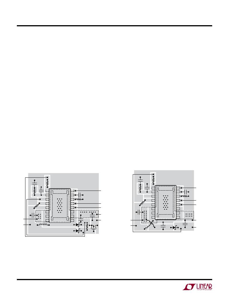
�Figure� 8.� Suggested� Component� Placement� for� Boost� Topology�
�(MSOP� Shown,� DFN� Similar,� Not� to� Scale.)� Pin� 15� on� DFN� or�
�Pin� 17� on� MSOP� Is� the� Exposed� Pad� Which� Must� Be� Soldered�
�Directly� to� the� Local� Ground� Plane� for� Adequate� Thermal�
�Performance.� Multiple� Vias� to� Additional� Ground� Planes� Will�
�Improve� Thermal� Performance�
�A:� RETURN� C� IN� AND� L2� GROUND� DIRECTLY� TO� LT3581� EXPOSED� PAD� PIN� 17.� IT� IS� ADVISED�
�TO� NOT� COMBINE� C� IN� AND� L2� GROUND� WITH� GND� EXCEPT� AT� THE� EXPOSED� PAD.�
�B:� RETURN� C� OUT� GROUNDS� DIRECTLY� TO� LT3581� EXPOSED� PAD� PIN� 17.� IT� IS� ADVISED�
�TO� NOT� COMBINE� C� OUT� GROUND� WITH� GND� EXCEPT� AT� THE� EXPOSED� PAD.�
�L1,� L2:� MOST� COUPLED� INDUCTOR� MANUFACTURERS� USE� CROSS� PINOUT� FOR� IMPROVED�
�PERFORMANCE.�
�Figure� 9.� Suggested� Component� Placement� for� SEPIC� Topology�
�(MSOP� Shown,� DFN� Similar,� Not� to� Scale.)� Pin� 15� on� DFN� or�
�Pin� 17� on� MSOP� Is� the� Exposed� Pad� Which� Must� Be� Soldered�
�Directly� to� the� Local� Ground� Plane� for� Adequate� Thermal�
�Performance.� Multiple� Vias� to� Additional� Ground� Planes� Will�
�Improve� Thermal� Performance�
�3581fa�
�16�
�For� more� information� www.linear.com/LT3581�
�相关PDF资料 |
PDF描述 |
|---|---|
| LT1777CS#PBF | IC REG BUCK ADJ 0.7A 16SOIC |
| EBA32DCBI | CONN EDGECARD 64POS R/A .125 SLD |
| 381LR121M400H032 | CAP ALUM 120UF 400V 20% SNAP |
| 2000-4R7-H-RC | INDUCTOR TOROID 4.7UH 20% HORZ |
| LTC3642EMS8E-3.3#PBF | IC REG BUCK SYNC 3.3V 50MA 8MSOP |
相关代理商/技术参数 |
参数描述 |
|---|---|
| LT3581EMSE-TRPBF | 制造商:LINER 制造商全称:Linear Technology 功能描述:3.3A Boost/Inverting DC/DC Converter with Fault Protection |
| LT3581HDE#PBF | 制造商:Linear Technology 功能描述:IC REG MULTI CONFIG ADJ 14DFN |
| LT3581HDE#TRPBF | 制造商:Linear Technology 功能描述:IC REG MULTI CONFIG ADJ 14DFN |
| LT3581IDE#PBF | 功能描述:IC REG MULTI CONFIG ADJ 14DFN RoHS:是 类别:集成电路 (IC) >> PMIC - 稳压器 - DC DC 开关稳压器 系列:- 标准包装:2,500 系列:- 类型:降压(降压) 输出类型:固定 输出数:1 输出电压:1.2V,1.5V,1.8V,2.5V 输入电压:2.7 V ~ 20 V PWM 型:- 频率 - 开关:- 电流 - 输出:50mA 同步整流器:是 工作温度:-40°C ~ 125°C 安装类型:表面贴装 封装/外壳:10-TFSOP,10-MSOP(0.118",3.00mm 宽)裸露焊盘 包装:带卷 (TR) 供应商设备封装:10-MSOP 裸露焊盘 |
| LT3581IDE#TRPBF | 功能描述:IC REG MULTI CONFIG ADJ 14DFN RoHS:是 类别:集成电路 (IC) >> PMIC - 稳压器 - DC DC 开关稳压器 系列:- 标准包装:2,500 系列:- 类型:降压(降压) 输出类型:固定 输出数:1 输出电压:1.2V,1.5V,1.8V,2.5V 输入电压:2.7 V ~ 20 V PWM 型:- 频率 - 开关:- 电流 - 输出:50mA 同步整流器:是 工作温度:-40°C ~ 125°C 安装类型:表面贴装 封装/外壳:10-TFSOP,10-MSOP(0.118",3.00mm 宽)裸露焊盘 包装:带卷 (TR) 供应商设备封装:10-MSOP 裸露焊盘 |
发布紧急采购,3分钟左右您将得到回复。