- 您现在的位置:买卖IC网 > PDF目录79850 > LT3757MPMSE#PBF (LINEAR TECHNOLOGY CORP) SWITCHING REGULATOR, 1000 kHz SWITCHING FREQ-MAX, PDSO10 PDF资料下载
参数资料
| 型号: | LT3757MPMSE#PBF |
| 厂商: | LINEAR TECHNOLOGY CORP |
| 元件分类: | 稳压器 |
| 英文描述: | SWITCHING REGULATOR, 1000 kHz SWITCHING FREQ-MAX, PDSO10 |
| 封装: | 3 X 3 MM, LEAD FREE, PLASTIC, MSOP-10 |
| 文件页数: | 10/36页 |
| 文件大小: | 436K |
| 代理商: | LT3757MPMSE#PBF |
第1页第2页第3页第4页第5页第6页第7页第8页第9页当前第10页第11页第12页第13页第14页第15页第16页第17页第18页第19页第20页第21页第22页第23页第24页第25页第26页第27页第28页第29页第30页第31页第32页第33页第34页第35页第36页
LT3757
18
3757fc
applicaTions inForMaTion
Flyback Converter: Switch Duty Cycle and Turns Ratio
The flyback converter conversion ratio in the continuous
mode operation is:
VOUT
VIN
=
NS
NP
D
1
D
where NS/NP is the second to primary turns ratio.
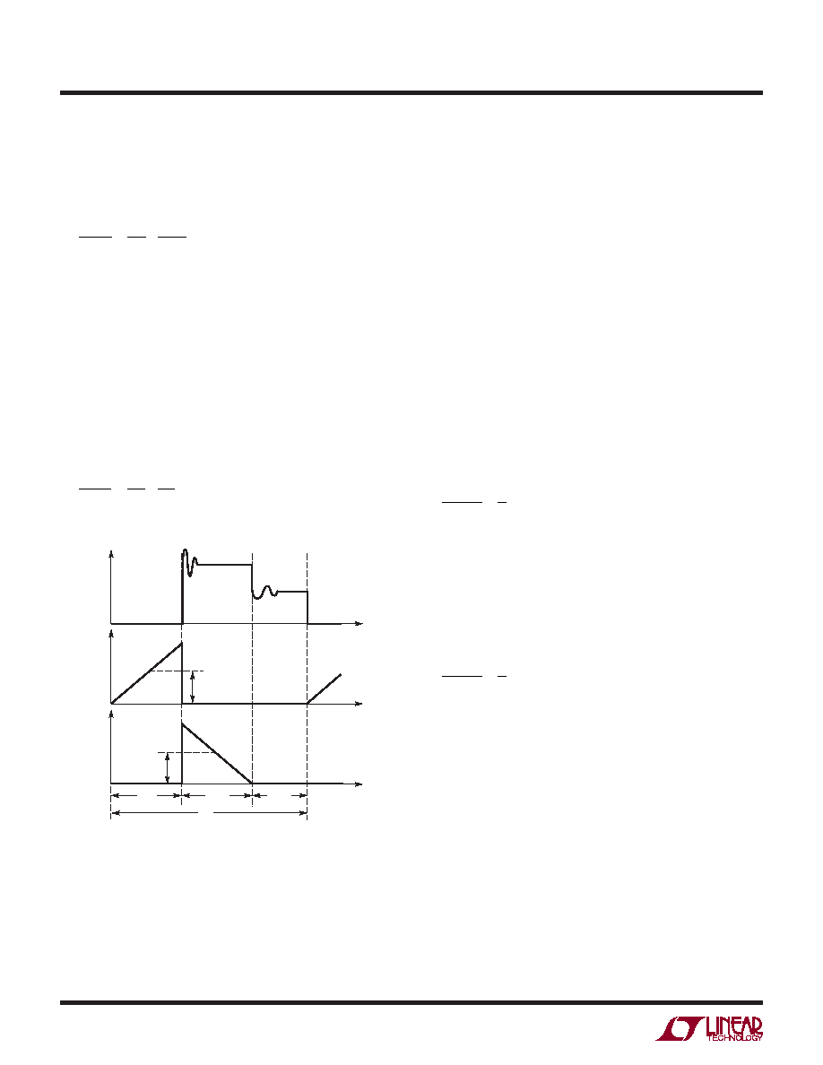
Figure 8 shows the waveforms of the flyback converter
in discontinuous mode operation. During each switching
period TS, three subintervals occur: DTS, D2TS, D3TS.
During DTS, M is on, and D is reverse-biased. During
D2TS, M is off, and LS is conducting current. Both LP and
LS currents are zero during D3TS.
The flyback converter conversion ratio in the discontinu-
ous mode operation is:
VOUT
VIN
=
NS
NP
D
D2
Accordingtotheprecedingequations,theuserhasrelative
freedom in selecting the switch duty cycle or turns ratio to
suit a given application. The selections of the duty cycle
and the turns ratio are somewhat iterative processes, due
to the number of variables involved. The user can choose
either a duty cycle or a turns ratio as the start point. The
following trade-offs should be considered when select-
ing the switch duty cycle or turns ratio, to optimize the
converter performance. A higher duty cycle affects the
flyback converter in the following aspects:
Lower MOSFET RMS current ISW(RMS), but higher
MOSFET VDS peak voltage
Lower diode peak reverse voltage, but higher diode
RMS current ID(RMS)
Higher transformer turns ratio (NP/NS)
The choice,
D
+D2
=
1
3
(for discontinuous mode operation with a given D3) gives
the power MOSFET the lowest power stress (the product
of RMS current and peak voltage). However, in the high
output voltage applications, a higher duty cycle may be
adopted to limit the large peak reverse voltage of the
diode. The choice,
D
+D2
=
2
3
(for discontinuous mode operation with a given D3) gives
the diode the lowest power stress (the product of RMS
current and peak voltage). An extreme high or low duty
cycle results in high power stress on the MOSFET or diode,
and reduces efficiency. It is recommended to choose a
duty cycle, D, between 20% and 80%.
Figure 8. Waveforms of the Flyback Converter
in Discontinuous Mode Operation
3757 F07
ISW
VDS
ID
t
DTS
D2TS
D3TS
ISW(MAX)
ID(MAX)
TS
相关PDF资料 |
PDF描述 |
|---|---|
| LM4040ESD-250GT3 | 1-OUTPUT TWO TERM VOLTAGE REFERENCE, 2.5 V, PDSO5 |
| LM4040DSD-330GT3 | 1-OUTPUT TWO TERM VOLTAGE REFERENCE, 3.3 V, PDSO5 |
| LM4040BIZ-5.0 | 1-OUTPUT TWO TERM VOLTAGE REFERENCE, 5 V, PBCY3 |
| LK5660-7EPD4TB1 | 2-OUTPUT 150 W AC-DC PWR FACTOR CORR MODULE |
| LT1374IR-5#TR | 8.5 A SWITCHING REGULATOR, 560 kHz SWITCHING FREQ-MAX, PSSO7 |
相关代理商/技术参数 |
参数描述 |
|---|---|
| LT3757MPMSE-TRPBF | 制造商:LINER 制造商全称:Linear Technology 功能描述:Boost, Flyback, SEPIC and Inverting Controller |
| LT3758 | 制造商:LINER 制造商全称:Linear Technology 功能描述:High Input Voltage, Boost, Flyback, SEPIC and Inverting Controller |
| LT3758A | 制造商:LINER 制造商全称:Linear Technology 功能描述:60V Low IQ Inverting DC/DC Controller Wide Operating VIN Range: 3.5V to 60V |
| LT3758AEDD#PBF | 制造商:Linear Technology 功能描述:IC REG CTRLR BST FLYBK INV 10DFN |
| LT3758AEDD#TRPBF | 制造商:Linear Technology 功能描述:IC REG CTRLR BST FLYBK INV 10DFN 制造商:Linear Technology 功能描述:SP-SWREG/Controller, High Input Voltage, Boost, Flyback, SEPIC and Inverting Con |
发布紧急采购,3分钟左右您将得到回复。